This thread has been locked.

If you have a related question, please click the "Ask a related question" button in the top right corner. The newly created question will be automatically linked to this question.

ADS8166: SPI Commuication between uC and ADC. No response on the MOSI line.

Part Number: ADS8166

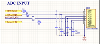
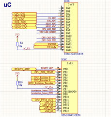
I'm having Problems to get the SPI Communication running between the uC and the ADS8166.

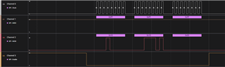
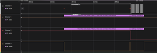
I am trying to read some register for test and have looked at the sent message on the MOSI line with a Logic Analyzer. The message actually looks exactly as described on p. 42 in the data sheet. But I don't get any response on the MISO line.

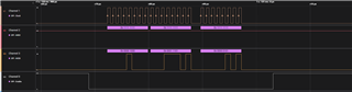
I try this sequence.
1. first I send the NOP bit (this is only because the communication does some strange things at the beginning and this was the try to give the IC time to initialize -> as shown in the screenshots)


2. then at which address I want to read
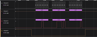

3. again a NOP bit.

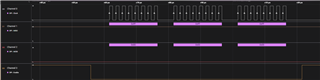
Actually I should now read the register 1D after the last message which should return only 0's because it is not initialized with anything.

Could you tell me if there could still be a problem with the message? Hardware technically I have ruled out an error in the meantime.

  • And I forgot to add this frame. This is the Read command. So this is sent between the write and the NOP frame I posted above.


  • Hi Matthias,

    Welcome to our e2e forum!  Sorry to hear that you are having issues with the ADS8166.  Can you please share your schematic with us?  In all of your LA plots above, it seems as though SDO is solidly held at logic 1, which seems strange to me.  Maybe we can see something in your schematic...  

  • Hello Tom. Sorry for my late reply.

    Here are the Schematics:


    I just found out, that I forgot to connect the RESET Pin of the ADC. So on my PCB I soldered 3V3 to the RESET Pin, but this did not solve the Problem. Also I found a layout misstake at Pin 4/5/6. But I also solved this. Now Pin 4 is connected to GND and C42/C43 are connected to GND on one side.

    Maybe this is helping you. 

  • Hi Matthias,

    Where are pins 21 and 31 tied?  I do not see these in your schematics, these pins need to go to ground.

  • Hi Tom,

    in the schematic these Pins are combined to keep the Design simple.


    This is the ADC on the PCB. 

  • OK - what voltages do you see on REFIO, REFP and REFby2?

  • REFIO: 8mV (so I guess there is nothing)
    REFP: 7.50mV (so I guess there is nothing)
    REFBY2: 4.5mV (so I guess there is nothing)

    Does this mean the IC is working correctly?

  • No, unfortunately.  There is an internal 4.096V reference that is powered ON by default, you should see that voltage on pin 3.  By default, the reference buffer is also enabled, so you should see 4.096 on REFP (pins 5-6) as well.  The REFby2 is also enabled by default so you should see 2.048V at pin 7.  Is the chip getting warm?  Can you verify the current draw for AVdd and DVdd?  I cant really make out your silkscreen, but is there a chance that the chip was rotated in the event the assembly folks thought your ground via between pins 8 and 9 was a 'Pin 1' indicator?

  • Hm. No the IC is not getting warm. 
    UnfortunatelyI don't have the measurement equipment to verify the current draw. But the Power Source of the PCB is not going in the Constant Current Mode and I have a total Current Consumption of 11mA-14mA.

    I assembled the IC by myself, so this is not a possibility.

  • I actually assembled more than one PCB. On the other PCB I am measuring 1.5V-2V on the REFIO Pin. 

    REFP and REFBY2 are still 0mV.

  • If you try to do a conversion on one of the grounded input channels, what do you see on SDO?

  • I still have the same behave. I attached my main.c . Maybe there is a misstake in it. Actually it's pretty simple and very basic to just read out one channel.

    3632.main.c
    /* USER CODE BEGIN Header */
    /**
      ******************************************************************************
      * @file           : main.c
      * @brief          : Main program body
      ******************************************************************************
      * @attention
      *
      * Copyright (c) 2023 STMicroelectronics.
      * All rights reserved.
      *
      * This software is licensed under terms that can be found in the LICENSE file
      * in the root directory of this software component.
      * If no LICENSE file comes with this software, it is provided AS-IS.
      *
      ******************************************************************************
      */
    /* USER CODE END Header */
    /* Includes ------------------------------------------------------------------*/
    #include "main.h"
    
    /* Private includes ----------------------------------------------------------*/
    /* USER CODE BEGIN Includes */
    #include "can.h"
    #include "sysTim_HAL.h"
    #include "adc_HAL_G4-Series.h"
    #include "stdio.h"
    #include "SPI.h"
    #include "ADS8166.h"
    #include "ADS8166_Register.h"
    #include "stdbool.h"
    #include "assert.h"
    
    
    /* USER CODE END Includes */
    
    /* Private typedef -----------------------------------------------------------*/
    /* USER CODE BEGIN PTD */
    /* USER CODE END PTD */
    
    /* Private define ------------------------------------------------------------*/
    /* USER CODE BEGIN PD */
    #define MAIN_ADS_WRITE_REGISTER 0b00001000
    #define SPI_WRITE 0b00001000
    #define SPI_READ 0b00010000
    #define SPI_NOP 0b00000000
    /* USER CODE END PD */
    
    /* Private macro -------------------------------------------------------------*/
    /* USER CODE BEGIN PM */
    
    /* USER CODE END PM */
    
    /* Private variables ---------------------------------------------------------*/
    ADC_HandleTypeDef hadc1;
    
    FDCAN_HandleTypeDef hfdcan1;
    
    I2C_HandleTypeDef hi2c1;
    
    SPI_HandleTypeDef hspi1;
    SPI_HandleTypeDef hspi2;
    
    TIM_HandleTypeDef htim2;
    
    /* USER CODE BEGIN PV */
    
    /* USER CODE END PV */
    
    /* Private function prototypes -----------------------------------------------*/
    void SystemClock_Config(void);
    static void MX_GPIO_Init(void);
    static void MX_ADC1_Init(void);
    static void MX_FDCAN1_Init(void);
    static void MX_I2C1_Init(void);
    static void MX_SPI1_Init(void);
    static void MX_SPI2_Init(void);
    static void MX_TIM2_Init(void);
    /* USER CODE BEGIN PFP */
    void initModules(void);
    void adc_startConversion();
    
    /* USER CODE END PFP */
    
    /* Private user code ---------------------------------------------------------*/
    /* USER CODE BEGIN 0 */
    void main_compose_write_command(uint8_t *data, uint16_t address, uint8_t value, uint8_t spi_command){
      data[0] = spi_command | (uint8_t)(address >> 8);
      data[1] = (uint8_t)(address);
      data[2] = value;
    }
    /* USER CODE END 0 */
    
    /**
      * @brief  The application entry point.
      * @retval int
      */
    int main(void)
    {
      /* USER CODE BEGIN 1 */
    
      /* USER CODE END 1 */
    
      /* MCU Configuration--------------------------------------------------------*/
    
      /* Reset of all peripherals, Initializes the Flash interface and the Systick. */
      HAL_Init();
    
      /* USER CODE BEGIN Init */
    
      /* USER CODE END Init */
    
      /* Configure the system clock */
      SystemClock_Config();
    
      /* USER CODE BEGIN SysInit */
    
      /* USER CODE END SysInit */
    
      /* Initialize all configured peripherals */
      MX_GPIO_Init();
      MX_ADC1_Init();
      MX_FDCAN1_Init();
      MX_I2C1_Init();
      MX_SPI1_Init();
      MX_SPI2_Init();
      MX_TIM2_Init();
      /* USER CODE BEGIN 2 */
    
      //TEST SPI
      HAL_GPIO_WritePin(SPI1_CS_GPIO_Port, SPI1_CS_Pin, GPIO_PIN_SET);
    //  HAL_GPIO_WritePin(READY_GPIO_Port, READY_Pin, GPIO_PIN_RESET);
    
    
    //  initModules();
    
    //  HAL_TIM_PWM_Start(&htim2, TIM_CHANNEL_4);		//Start PWM
    
     uint8_t data[3] = {0, 0, 0};
    
    
       uint8_t receivedata[3] = {0, 0, 0};
    
    
     /* main_compose_write_command(data, 0, 0, SPI_NOP);
    
      HAL_GPIO_WritePin(SPI1_CS_GPIO_Port, SPI1_CS_Pin, GPIO_PIN_RESET);
      HAL_SPI_Transmit(&hspi1, (uint8_t*)&data, 3, 10);
      HAL_GPIO_WritePin(SPI1_CS_GPIO_Port, SPI1_CS_Pin, GPIO_PIN_SET);
      */
    //  HAL_Delay(1);
    /*
      main_compose_write_command(data, 0x1D, 0x01, SPI_WRITE);
    //  main_compose_write_command(data, 0x1D, 0x00, SPI_WRITE);
    
      HAL_GPIO_WritePin(SPI1_CS_GPIO_Port, SPI1_CS_Pin, GPIO_PIN_RESET);
      HAL_SPI_Transmit(&hspi1, (uint8_t*)&data, 3, 10);
      HAL_GPIO_WritePin(SPI1_CS_GPIO_Port, SPI1_CS_Pin, GPIO_PIN_SET);
    //  HAL_Delay(1);
    
      main_compose_write_command(data, 0x1D, 0x06, SPI_READ);
    //  main_compose_write_command(data, 0x00, 0x00, SPI_NOP);
    
      HAL_GPIO_WritePin(SPI1_CS_GPIO_Port, SPI1_CS_Pin, GPIO_PIN_RESET);
      HAL_SPI_Transmit(&hspi1, (uint8_t*)&data, 3, 10);
      HAL_GPIO_WritePin(SPI1_CS_GPIO_Port, SPI1_CS_Pin, GPIO_PIN_SET);
    //  HAL_Delay(1);
    
      main_compose_write_command(data, 0, 0, SPI_NOP);*/
    
    //  HAL_Delay(1);
    
    //   __HAL_TIM_SET_COMPARE(&htim2, TIM_CHANNEL_2, 50);
    
      /* USER CODE END 2 */
    
      /* Infinite loop */
      /* USER CODE BEGIN WHILE */
      while (1)
      {
    	  main_compose_write_command(data, 0x1D, 0x05, SPI_WRITE);
    	  HAL_GPIO_WritePin(SPI1_CS_GPIO_Port, SPI1_CS_Pin, GPIO_PIN_RESET);
    	  HAL_SPI_TransmitReceive(&hspi1, data, receivedata, 3,10);
    	  HAL_GPIO_WritePin(SPI1_CS_GPIO_Port, SPI1_CS_Pin, GPIO_PIN_SET);
    	  HAL_Delay(1);
    
    	  main_compose_write_command(data, 0x1D, 0x00, SPI_WRITE);
    	  HAL_GPIO_WritePin(SPI1_CS_GPIO_Port, SPI1_CS_Pin, GPIO_PIN_RESET);
    	  HAL_SPI_TransmitReceive(&hspi1, data, receivedata, 3,10);
    	  HAL_GPIO_WritePin(SPI1_CS_GPIO_Port, SPI1_CS_Pin, GPIO_PIN_SET);
    	  HAL_Delay(1);
    
    	  main_compose_write_command(data, 0, 0, SPI_NOP);
    
    	  HAL_GPIO_WritePin(SPI1_CS_GPIO_Port, SPI1_CS_Pin, GPIO_PIN_RESET);
    	  HAL_SPI_TransmitReceive(&hspi1, data, receivedata, 3,10);
    	  HAL_GPIO_WritePin(SPI1_CS_GPIO_Port, SPI1_CS_Pin, GPIO_PIN_SET);
    
    	  HAL_Delay(1);
    
        /* USER CODE END WHILE */
    
        /* USER CODE BEGIN 3 */
      }
      /* USER CODE END 3 */
    }
    
    /**
      * @brief System Clock Configuration
      * @retval None
      */
    void SystemClock_Config(void)
    {
      RCC_OscInitTypeDef RCC_OscInitStruct = {0};
      RCC_ClkInitTypeDef RCC_ClkInitStruct = {0};
    
      /** Configure the main internal regulator output voltage
      */
      HAL_PWREx_ControlVoltageScaling(PWR_REGULATOR_VOLTAGE_SCALE1);
    
      /** Initializes the RCC Oscillators according to the specified parameters
      * in the RCC_OscInitTypeDef structure.
      */
      RCC_OscInitStruct.OscillatorType = RCC_OSCILLATORTYPE_HSE;
      RCC_OscInitStruct.HSEState = RCC_HSE_ON;
      RCC_OscInitStruct.PLL.PLLState = RCC_PLL_ON;
      RCC_OscInitStruct.PLL.PLLSource = RCC_PLLSOURCE_HSE;
      RCC_OscInitStruct.PLL.PLLM = RCC_PLLM_DIV1;
      RCC_OscInitStruct.PLL.PLLN = 16;
      RCC_OscInitStruct.PLL.PLLP = RCC_PLLP_DIV2;
      RCC_OscInitStruct.PLL.PLLQ = RCC_PLLQ_DIV2;
      RCC_OscInitStruct.PLL.PLLR = RCC_PLLR_DIV2;
      if (HAL_RCC_OscConfig(&RCC_OscInitStruct) != HAL_OK)
      {
        Error_Handler();
      }
    
      /** Initializes the CPU, AHB and APB buses clocks
      */
      RCC_ClkInitStruct.ClockType = RCC_CLOCKTYPE_HCLK|RCC_CLOCKTYPE_SYSCLK
                                  |RCC_CLOCKTYPE_PCLK1|RCC_CLOCKTYPE_PCLK2;
      RCC_ClkInitStruct.SYSCLKSource = RCC_SYSCLKSOURCE_PLLCLK;
      RCC_ClkInitStruct.AHBCLKDivider = RCC_SYSCLK_DIV1;
      RCC_ClkInitStruct.APB1CLKDivider = RCC_HCLK_DIV1;
      RCC_ClkInitStruct.APB2CLKDivider = RCC_HCLK_DIV1;
    
      if (HAL_RCC_ClockConfig(&RCC_ClkInitStruct, FLASH_LATENCY_4) != HAL_OK)
      {
        Error_Handler();
      }
    }
    
    /**
      * @brief ADC1 Initialization Function
      * @param None
      * @retval None
      */
    static void MX_ADC1_Init(void)
    {
    
      /* USER CODE BEGIN ADC1_Init 0 */
    
      /* USER CODE END ADC1_Init 0 */
    
      ADC_MultiModeTypeDef multimode = {0};
      ADC_ChannelConfTypeDef sConfig = {0};
    
      /* USER CODE BEGIN ADC1_Init 1 */
    
      /* USER CODE END ADC1_Init 1 */
    
      /** Common config
      */
      hadc1.Instance = ADC1;
      hadc1.Init.ClockPrescaler = ADC_CLOCK_SYNC_PCLK_DIV4;
      hadc1.Init.Resolution = ADC_RESOLUTION_12B;
      hadc1.Init.DataAlign = ADC_DATAALIGN_RIGHT;
      hadc1.Init.GainCompensation = 0;
      hadc1.Init.ScanConvMode = ADC_SCAN_DISABLE;
      hadc1.Init.EOCSelection = ADC_EOC_SINGLE_CONV;
      hadc1.Init.LowPowerAutoWait = DISABLE;
      hadc1.Init.ContinuousConvMode = DISABLE;
      hadc1.Init.NbrOfConversion = 1;
      hadc1.Init.DiscontinuousConvMode = DISABLE;
      hadc1.Init.ExternalTrigConv = ADC_SOFTWARE_START;
      hadc1.Init.ExternalTrigConvEdge = ADC_EXTERNALTRIGCONVEDGE_NONE;
      hadc1.Init.DMAContinuousRequests = DISABLE;
      hadc1.Init.Overrun = ADC_OVR_DATA_PRESERVED;
      hadc1.Init.OversamplingMode = DISABLE;
      if (HAL_ADC_Init(&hadc1) != HAL_OK)
      {
        Error_Handler();
      }
    
      /** Configure the ADC multi-mode
      */
      multimode.Mode = ADC_MODE_INDEPENDENT;
      if (HAL_ADCEx_MultiModeConfigChannel(&hadc1, &multimode) != HAL_OK)
      {
        Error_Handler();
      }
    
      /** Configure Regular Channel
      */
      sConfig.Channel = ADC_CHANNEL_12;
      sConfig.Rank = ADC_REGULAR_RANK_1;
      sConfig.SamplingTime = ADC_SAMPLETIME_2CYCLES_5;
      sConfig.SingleDiff = ADC_SINGLE_ENDED;
      sConfig.OffsetNumber = ADC_OFFSET_NONE;
      sConfig.Offset = 0;
      if (HAL_ADC_ConfigChannel(&hadc1, &sConfig) != HAL_OK)
      {
        Error_Handler();
      }
      /* USER CODE BEGIN ADC1_Init 2 */
    
      /* USER CODE END ADC1_Init 2 */
    
    }
    
    /**
      * @brief FDCAN1 Initialization Function
      * @param None
      * @retval None
      */
    static void MX_FDCAN1_Init(void)
    {
    
      /* USER CODE BEGIN FDCAN1_Init 0 */
    
      /* USER CODE END FDCAN1_Init 0 */
    
      /* USER CODE BEGIN FDCAN1_Init 1 */
    
      /* USER CODE END FDCAN1_Init 1 */
      hfdcan1.Instance = FDCAN1;
      hfdcan1.Init.ClockDivider = FDCAN_CLOCK_DIV1;
      hfdcan1.Init.FrameFormat = FDCAN_FRAME_CLASSIC;
      hfdcan1.Init.Mode = FDCAN_MODE_NORMAL;
      hfdcan1.Init.AutoRetransmission = ENABLE;
      hfdcan1.Init.TransmitPause = DISABLE;
      hfdcan1.Init.ProtocolException = DISABLE;
      hfdcan1.Init.NominalPrescaler = 4;
      hfdcan1.Init.NominalSyncJumpWidth = 1;
      hfdcan1.Init.NominalTimeSeg1 = 13;
      hfdcan1.Init.NominalTimeSeg2 = 4;
      hfdcan1.Init.DataPrescaler = 1;
      hfdcan1.Init.DataSyncJumpWidth = 1;
      hfdcan1.Init.DataTimeSeg1 = 13;
      hfdcan1.Init.DataTimeSeg2 = 2;
      hfdcan1.Init.StdFiltersNbr = 1;
      hfdcan1.Init.ExtFiltersNbr = 0;
      hfdcan1.Init.TxFifoQueueMode = FDCAN_TX_FIFO_OPERATION;
      if (HAL_FDCAN_Init(&hfdcan1) != HAL_OK)
      {
        Error_Handler();
      }
      /* USER CODE BEGIN FDCAN1_Init 2 */
    
    
      /* USER CODE END FDCAN1_Init 2 */
    
    }
    
    /**
      * @brief I2C1 Initialization Function
      * @param None
      * @retval None
      */
    static void MX_I2C1_Init(void)
    {
    
      /* USER CODE BEGIN I2C1_Init 0 */
    
      /* USER CODE END I2C1_Init 0 */
    
      /* USER CODE BEGIN I2C1_Init 1 */
    
      /* USER CODE END I2C1_Init 1 */
      hi2c1.Instance = I2C1;
      hi2c1.Init.Timing = 0x20A0C4DF;
      hi2c1.Init.OwnAddress1 = 0;
      hi2c1.Init.AddressingMode = I2C_ADDRESSINGMODE_7BIT;
      hi2c1.Init.DualAddressMode = I2C_DUALADDRESS_DISABLE;
      hi2c1.Init.OwnAddress2 = 0;
      hi2c1.Init.OwnAddress2Masks = I2C_OA2_NOMASK;
      hi2c1.Init.GeneralCallMode = I2C_GENERALCALL_DISABLE;
      hi2c1.Init.NoStretchMode = I2C_NOSTRETCH_DISABLE;
      if (HAL_I2C_Init(&hi2c1) != HAL_OK)
      {
        Error_Handler();
      }
    
      /** Configure Analogue filter
      */
      if (HAL_I2CEx_ConfigAnalogFilter(&hi2c1, I2C_ANALOGFILTER_ENABLE) != HAL_OK)
      {
        Error_Handler();
      }
    
      /** Configure Digital filter
      */
      if (HAL_I2CEx_ConfigDigitalFilter(&hi2c1, 0) != HAL_OK)
      {
        Error_Handler();
      }
      /* USER CODE BEGIN I2C1_Init 2 */
    
      /* USER CODE END I2C1_Init 2 */
    
    }
    
    /**
      * @brief SPI1 Initialization Function
      * @param None
      * @retval None
      */
    static void MX_SPI1_Init(void)
    {
    
      /* USER CODE BEGIN SPI1_Init 0 */
    
      /* USER CODE END SPI1_Init 0 */
    
      /* USER CODE BEGIN SPI1_Init 1 */
    
      /* USER CODE END SPI1_Init 1 */
      /* SPI1 parameter configuration*/
      hspi1.Instance = SPI1;
      hspi1.Init.Mode = SPI_MODE_MASTER;
      hspi1.Init.Direction = SPI_DIRECTION_2LINES;
      hspi1.Init.DataSize = SPI_DATASIZE_8BIT;
      hspi1.Init.CLKPolarity = SPI_POLARITY_LOW;
      hspi1.Init.CLKPhase = SPI_PHASE_1EDGE;
      hspi1.Init.NSS = SPI_NSS_SOFT;
      hspi1.Init.BaudRatePrescaler = SPI_BAUDRATEPRESCALER_128;
      hspi1.Init.FirstBit = SPI_FIRSTBIT_MSB;
      hspi1.Init.TIMode = SPI_TIMODE_DISABLE;
      hspi1.Init.CRCCalculation = SPI_CRCCALCULATION_DISABLE;
      hspi1.Init.CRCPolynomial = 7;
      hspi1.Init.CRCLength = SPI_CRC_LENGTH_DATASIZE;
      hspi1.Init.NSSPMode = SPI_NSS_PULSE_DISABLE;
      if (HAL_SPI_Init(&hspi1) != HAL_OK)
      {
        Error_Handler();
      }
      /* USER CODE BEGIN SPI1_Init 2 */
    
      /* USER CODE END SPI1_Init 2 */
    
    }
    
    /**
      * @brief SPI2 Initialization Function
      * @param None
      * @retval None
      */
    static void MX_SPI2_Init(void)
    {
    
      /* USER CODE BEGIN SPI2_Init 0 */
    
      /* USER CODE END SPI2_Init 0 */
    
      /* USER CODE BEGIN SPI2_Init 1 */
    
      /* USER CODE END SPI2_Init 1 */
      /* SPI2 parameter configuration*/
      hspi2.Instance = SPI2;
      hspi2.Init.Mode = SPI_MODE_MASTER;
      hspi2.Init.Direction = SPI_DIRECTION_2LINES;
      hspi2.Init.DataSize = SPI_DATASIZE_4BIT;
      hspi2.Init.CLKPolarity = SPI_POLARITY_LOW;
      hspi2.Init.CLKPhase = SPI_PHASE_1EDGE;
      hspi2.Init.NSS = SPI_NSS_HARD_OUTPUT;
      hspi2.Init.BaudRatePrescaler = SPI_BAUDRATEPRESCALER_2;
      hspi2.Init.FirstBit = SPI_FIRSTBIT_MSB;
      hspi2.Init.TIMode = SPI_TIMODE_DISABLE;
      hspi2.Init.CRCCalculation = SPI_CRCCALCULATION_DISABLE;
      hspi2.Init.CRCPolynomial = 7;
      hspi2.Init.CRCLength = SPI_CRC_LENGTH_DATASIZE;
      hspi2.Init.NSSPMode = SPI_NSS_PULSE_ENABLE;
      if (HAL_SPI_Init(&hspi2) != HAL_OK)
      {
        Error_Handler();
      }
      /* USER CODE BEGIN SPI2_Init 2 */
    
      /* USER CODE END SPI2_Init 2 */
    
    }
    
    /**
      * @brief TIM2 Initialization Function
      * @param None
      * @retval None
      */
    static void MX_TIM2_Init(void)
    {
    
      /* USER CODE BEGIN TIM2_Init 0 */
    
      /* USER CODE END TIM2_Init 0 */
    
      TIM_MasterConfigTypeDef sMasterConfig = {0};
      TIM_OC_InitTypeDef sConfigOC = {0};
    
      /* USER CODE BEGIN TIM2_Init 1 */
    
      /* USER CODE END TIM2_Init 1 */
      htim2.Instance = TIM2;
      htim2.Init.Prescaler = 6;
      htim2.Init.CounterMode = TIM_COUNTERMODE_UP;
      htim2.Init.Period = 30000;
      htim2.Init.ClockDivision = TIM_CLOCKDIVISION_DIV1;
      htim2.Init.AutoReloadPreload = TIM_AUTORELOAD_PRELOAD_DISABLE;
      if (HAL_TIM_PWM_Init(&htim2) != HAL_OK)
      {
        Error_Handler();
      }
      sMasterConfig.MasterOutputTrigger = TIM_TRGO_RESET;
      sMasterConfig.MasterSlaveMode = TIM_MASTERSLAVEMODE_DISABLE;
      if (HAL_TIMEx_MasterConfigSynchronization(&htim2, &sMasterConfig) != HAL_OK)
      {
        Error_Handler();
      }
      sConfigOC.OCMode = TIM_OCMODE_PWM1;
      sConfigOC.Pulse = 0;
      sConfigOC.OCPolarity = TIM_OCPOLARITY_HIGH;
      sConfigOC.OCFastMode = TIM_OCFAST_DISABLE;
      if (HAL_TIM_PWM_ConfigChannel(&htim2, &sConfigOC, TIM_CHANNEL_4) != HAL_OK)
      {
        Error_Handler();
      }
      /* USER CODE BEGIN TIM2_Init 2 */
    
      /* USER CODE END TIM2_Init 2 */
      HAL_TIM_MspPostInit(&htim2);
    
    }
    
    /**
      * @brief GPIO Initialization Function
      * @param None
      * @retval None
      */
    static void MX_GPIO_Init(void)
    {
      GPIO_InitTypeDef GPIO_InitStruct = {0};
    /* USER CODE BEGIN MX_GPIO_Init_1 */
    /* USER CODE END MX_GPIO_Init_1 */
    
      /* GPIO Ports Clock Enable */
      __HAL_RCC_GPIOF_CLK_ENABLE();
      __HAL_RCC_GPIOA_CLK_ENABLE();
      __HAL_RCC_GPIOB_CLK_ENABLE();
    
      /*Configure GPIO pin Output Level */
      HAL_GPIO_WritePin(GPIOA, CPU_GS0_Pin|CPU_GS1_Pin|CPU_LED_RED_Pin|CPU_LED_GREEN_Pin, GPIO_PIN_RESET);
    
      /*Configure GPIO pin Output Level */
      HAL_GPIO_WritePin(SPI1_CS_GPIO_Port, SPI1_CS_Pin, GPIO_PIN_SET);
    
      /*Configure GPIO pin Output Level */
      HAL_GPIO_WritePin(READY_GPIO_Port, READY_Pin, GPIO_PIN_RESET);
    
      /*Configure GPIO pins : CPU_GS0_Pin CPU_GS1_Pin CPU_LED_RED_Pin CPU_LED_GREEN_Pin */
      GPIO_InitStruct.Pin = CPU_GS0_Pin|CPU_GS1_Pin|CPU_LED_RED_Pin|CPU_LED_GREEN_Pin;
      GPIO_InitStruct.Mode = GPIO_MODE_OUTPUT_PP;
      GPIO_InitStruct.Pull = GPIO_NOPULL;
      GPIO_InitStruct.Speed = GPIO_SPEED_FREQ_LOW;
      HAL_GPIO_Init(GPIOA, &GPIO_InitStruct);
    
      /*Configure GPIO pin : SPI1_CS_Pin */
      GPIO_InitStruct.Pin = SPI1_CS_Pin;
      GPIO_InitStruct.Mode = GPIO_MODE_OUTPUT_PP;
      GPIO_InitStruct.Pull = GPIO_NOPULL;
      GPIO_InitStruct.Speed = GPIO_SPEED_FREQ_HIGH;
      HAL_GPIO_Init(SPI1_CS_GPIO_Port, &GPIO_InitStruct);
    
      /*Configure GPIO pin : READY_Pin */
      GPIO_InitStruct.Pin = READY_Pin;
      GPIO_InitStruct.Mode = GPIO_MODE_OUTPUT_PP;
      GPIO_InitStruct.Pull = GPIO_NOPULL;
      GPIO_InitStruct.Speed = GPIO_SPEED_FREQ_LOW;
      HAL_GPIO_Init(READY_GPIO_Port, &GPIO_InitStruct);
    
      /*Configure GPIO pins : CPU_Encoder_B_Pin CPU_Encoder_A_Pin CPU_Rotation_Encoder_Pin */
      GPIO_InitStruct.Pin = CPU_Encoder_B_Pin|CPU_Encoder_A_Pin|CPU_Rotation_Encoder_Pin;
      GPIO_InitStruct.Mode = GPIO_MODE_INPUT;
      GPIO_InitStruct.Pull = GPIO_NOPULL;
      HAL_GPIO_Init(GPIOB, &GPIO_InitStruct);
    
      /*Configure GPIO pins : Acceleration_Sensor_INT2_Pin Acceleration_Sensor_INT1_Pin */
      GPIO_InitStruct.Pin = Acceleration_Sensor_INT2_Pin|Acceleration_Sensor_INT1_Pin;
      GPIO_InitStruct.Mode = GPIO_MODE_IT_RISING;
      GPIO_InitStruct.Pull = GPIO_NOPULL;
      HAL_GPIO_Init(GPIOB, &GPIO_InitStruct);
    
    /* USER CODE BEGIN MX_GPIO_Init_2 */
    /* USER CODE END MX_GPIO_Init_2 */
    }
    
    /* USER CODE BEGIN 4 */
    void initModules(void){
    	can_init(&hfdcan1);
    	adc_startConversion(&hadc1);
    	SPI_init(&hspi1);
    //	init_ADS8166();
    
    	sysTim_addTask(can_heartbeatFunction, 1000);
    
    }
    
    
    /* USER CODE END 4 */
    
    /**
      * @brief  This function is executed in case of error occurrence.
      * @retval None
      */
    void Error_Handler(void)
    {
      /* USER CODE BEGIN Error_Handler_Debug */
      /* User can add his own implementation to report the HAL error return state */
      __disable_irq();
      while (1)
      {
      }
      /* USER CODE END Error_Handler_Debug */
    }
    
    #ifdef  USE_FULL_ASSERT
    /**
      * @brief  Reports the name of the source file and the source line number
      *         where the assert_param error has occurred.
      * @param  file: pointer to the source file name
      * @param  line: assert_param error line source number
      * @retval None
      */
    void assert_failed(uint8_t *file, uint32_t line)
    {
      /* USER CODE BEGIN 6 */
      /* User can add his own implementation to report the file name and line number,
         ex: printf("Wrong parameters value: file %s on line %d\r\n", file, line) */
      /* USER CODE END 6 */
    }
    #endif /* USE_FULL_ASSERT */
    

  • And this is the data of the LA to this Code Section:

  • So, that looks like a write to the CHANNEL_ID Register asking for AIN5.  From there, you should be able to toggle /CS, send 0x00 through SDI and read back from SDO.  I've no idea at the moment while all you get back on the SDO line is 0xFF.