This thread has been locked.

If you have a related question, please click the "Ask a related question" button in the top right corner. The newly created question will be automatically linked to this question.

DAC8830: Understanding the Power-On Reset and possible causes for unpredictable Start-up Value

Part Number: DAC8830

The datasheet states in the section titled Power-On Reset on page 16 that "After power-up, the output from pin VOUT of the DAC8830 is 0 V."

In our hardware we have found this statement to not always hold true. After bootup our DAC8830 VDD pin has 5V, the reference reaches 5V, and when we start communicating with the DAC, we have the expected SPI based control of Vout. However, at power on and before communication, sometimes the DAC will power on with Vout = 0V and other times the DAC comes up with Vout = 5V or 2.5V or 3.4V. We are using 16 of these DACs in the system and each has its own stable output voltage that it will go to when we boot into this "wrong state". I have verified that our SPI CLK is quiet except for a single rising edge on power-up, do to a design choice that idles the clk high. I assume this means that I can't be loading in a non-zero value in to the DACs until my intended communication begins.

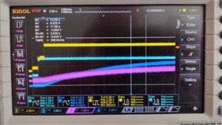
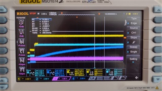
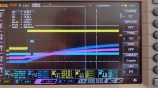
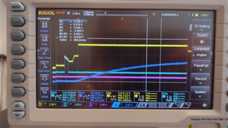
The only difference I can find between when the DAC starts with Vout = 0V and Vout equaling some other voltage, has to do with our voltage reference which has a very slow time constant of 10 seconds. When the reference is stable, 5V, and we reboot the system, then Vout = 0V on every DAC. Note that the reboot process does not give enough time to bleed off the voltage reference, so when the DAC powers after reboot the 5V reference is present. However, when the system is turned on for the first time after a long wait, 30s, then Vout rises in sync with Vref until Vout reaches the non-zero start-up value. Since Vref needs 10s to get to 70% of 5V, it is not present during the power on sequence in the cold start case.

So my question is this, how is the POR achieved and could the absence of Vref at power on somehow thwart the function of the POR? or is there some other reason the DAC might start with a non-zero Vout?

Any help is appreciated.

  • Erin will review this and respond.

  • Hi Scott,

    I'm looking into this now, thank you for your patience.

    Thanks,
    Erin

  • Hi Scott,

    Some questions from our design team: What is your power on sequence? Does the power for your digital pins come on before or after the VDD supply? 

    Alongside this, it would be helpful to see some scope screenshots of the supply ramp up in both situations. A screenshot with VDD, SCLK, VREF, and VOUT, showing one situation with VREF already on and one with VREF ramping up would be useful in seeing if we can pinpoint the issue.

    Thanks,
    Erin

  • Thanks Erin.

    It will take a while to get you screenshots, but I can give you the expected behavior now.

    Power up sequence from a cold start:

    1. Power is applied to the system
    2. About 1ms later the 5V analog rail powers on at the DAC.
    3. About 1.5ms later (2.5ms total) the 3.3V digital rail powers on at the DAC.
    4. About 8.5ms later (11ms total) the 5V reference powers up at the DAC.

    When rebooting the system the 5V reference ,line #4, does not have time discharge and so it is already mostly at 5V when power is first applied.

  • And in this case for the cold start, this is where you see the DACs behave incorrectly? Where they have a voltage other than 0V?

  • The Cold Start has the incorrect behavior, Vout does not equal 0V, and the Reboot has the correct behavior, Vout=0V.

    Here are the O-scope captures of the two traces. Yellow is the 5V VDD rail. Cyan is the CLK, Blue is Vref, and Magenta is Vout. The timescale is 2 sec per divide and the 2V vertically.

    Cold Start Reboot

    A few things stick out to me.

    1. I messed up a unit from my timing statement before. The Vref signal is a 10s time constant not 10ms time constant. Sorry about that.
    2. The Vref gets lower than I originally thought. However it is still the big difference. During a Reboot Vref has a sharp step caused when the opamp in the reference turns on and passes the non-zero Vref through (this is the step right after the Cyan step and unfortunately is mostly hidden by the Vout, Magenta, trace). The Cold Start has just the charging capacitor curve which no sharp edge.
  • Hi Scott,

    I'd like to confirm, yellow is VDD and Cyan is CLK? Looks like digital would be coming on before analog then. Additionally, it looks like your VDD is raising in a 2 step ramp. It raises to 2V with SCLK, then raises the additional 2V a few milliseconds after. Is this expected in your system? This may present an issue if the device is not being powered properly.

    Thanks for the screenshots! Will let you know of any other information the designers and I dig up.

    Thanks,
    Erin

  • Hi Scott,

    The designers would like to try a power up sequence while keeping the SCLK low. The shift registers don't clear upon a power up reset, and with a high clock edge the device could potentially be pushing data into the DAC registers. Is it possible for you to do the Cold Start powerup sequence with SCLK held low?

    Thanks,
    Erin

  • You are correct, Yellow is VDD and Cyan is CLK.

    The two step power is surprising. I know of no part of my circuit that should produce that behavior. It is possible that the CLK is actually powering the chip until VDD goes high VDD is 1V lower than CLK during that time? I have power delays that should set that order the other way but let me try changing some values to correct that behavior and get back to you....

    Okay those changes did nothing and I my rails should be forced to come up in the reverse order. Something strange is going on here that I will have to look into further tomorrow. 

  • I spent all day tracking this one down, but I have a patch for now. We cannot remove the CLK edge sent to the DAC8830 as it is the byproduct of the FPGA Pin going high during configuration. I don't know why this pin goes high, but we can find no way to stop it from happening. The best we can do is pull the output back low once configuration is complete. Adding this second edge actually makes the problem worse, however, making the Vout always power on in an unknown state, at least if the power is applied before the CLK pulse arrives. As you can see in the trace below, VDD goes high before the CLK pulse is received and Vout then ramps with Vref.

    However, if I wait to power the chip until after the CLK pulse is sent then the chip powers on in the correct Vout=0V state, Magenta, during both Cold Starts and Reboots. This means that I'm parasitically powering the chip from the SCLK line during the pulse and possibly through other ICs on the board but it does remove the startup uncertainty. I would call that an unattractive solution, but it is a solution.

    Has you team come up with an other way to avoid the start-up uncertainty problem? Do they know what side effects I may encounter if I use my patched solution permanently, i.e. a shortened chip life?

  • Glad to see there's a solution to the problem. Here's another test design wants to try:

    What's the status of your CS line at startup? If it's low, then it's likely the issue is indeed with the SCLK loading in faulty data at startup. Could you try holding CS high before powering up to see if that also solves the problem? 

    I'll ask the designers about your patched solution in case holding CS high doesn't work. I don't foresee any issues with the SCLK pulse before powerup, but I'll double check to make sure.

  • Thanks for checking my solution with your team.

    We don't have control of the CS any more than the SCLK during FPGA configuration, so if it is low, I can't do anything about it.  I'll still do the test, but the system is needed for other tests so this one will take longer to work in. If it is low I'll have to hard-wire it high to accomplish what your design team wants which is not a working state for the system.

  • Hi Scott,

    Design has some concerns with powering SCLK with the pulse before VDD, as the digital line isn't meant to be a higher than 0.3V + VDD. Is your CS line powered through the FPGA as well? If so, it might be nice to see a scope screenshot of that as well, to see how it aligns with SCLK. 

    Another potential solution, if you can't control the CS pin (or if raising that high doesn't work): Could you power on VDD before the SCLK pulse, then take them both to 0V? Then start up the part normally with VDD and VREF. This would protect the part from being powered by SCLK, and if your VREF is 0V then you shouldn't see any DAC output. I'm not sure if this is possible on your setup, but it would be a safer solution than just letting SCLK pulse before powerup.

    Thanks,
    Erin