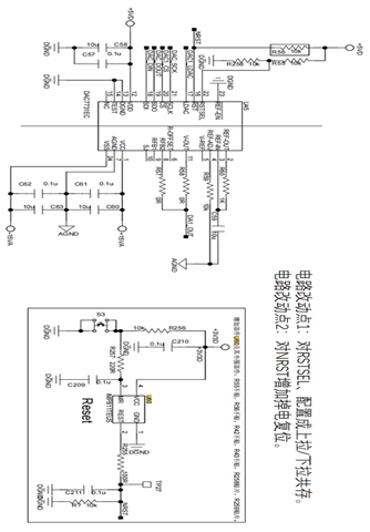
This thread has been locked.

If you have a related question, please click the "Ask a related question" button in the top right corner. The newly created question will be automatically linked to this question.

DAC7731: how to configure pins 16 and 22.

Part Number: DAC7731

Dear Expert

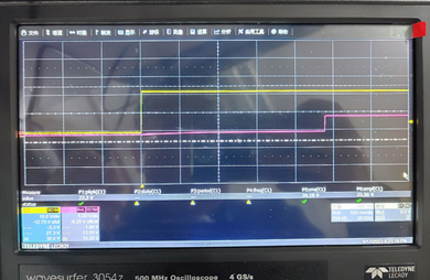
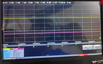
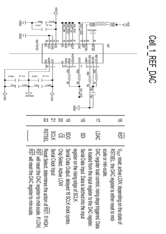
This is the schematic diagram before the change. We tested that applying surge interference would cause abnormal output of pin 11 .

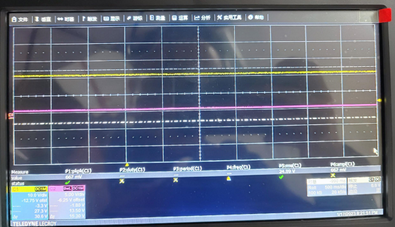
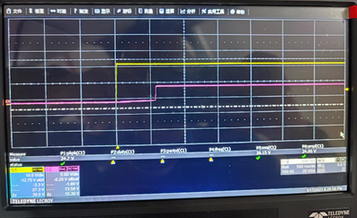
The customer changed RSTSEL to add a pull-down 10K resistor, and RST to add a power down reset output low-level IC. Surge interference does not affect pin 11, and the output signal of pin 11 is normal.
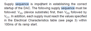
May I ask why this phenomenon is caused by making such changes to the PIN16 and PIN22 pins controlled by the chip? I would like to consult FAE on how to configure pins 16 and 22.

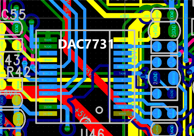
Below is pcb layout :

  • Hi Gabriel,

    Can you please provide some more detail regarding the surge interference, where and how you applying it? 

    Meantime, I will look the design.


    Thanks,

    Sanjay 

  • Dear Sanjay

    Through analysis, it was found that there is a significant difference in the signal output of the DAC7731 when the power on timing of the 5V power supply and the 24V power supply is different. We found when the reset time is sufficient, the power on output is normal.

    1)When powered on, there is a difference of 2.4s between 24V and 5V. In this case, the DACout output is about 1.9V after power on (This is abnormal condition).

    2)When powered on, the difference between 24V and 5V is about 0.6s. In this case, after power on, the DACout output is about -5V (This is normal condition).

    By analyzing the schematic diagram and specifications, it was found that the reset setting pin and reset pin design of DAC7731 are unreliable in the current design. When the reset time is insufficient, there may be situations where the internal configuration is incorrect and the power output is abnormal. When the reset time is sufficient, the power on output is normal.

    According to the specifications and schematic diagram, when the 22 pin of the DAC7731 is pulled up, the DAC will be powered on_ Out output is 0V, when 22 feet are pulled, after power on, DAC_ Out output is -10V (TP1 TP2 output is -5V).
    The voltage of TP1 TP2 on a normal circuit board is -5V after power on, while the voltage of TP1 TP2 on an abnormal circuit board is -2.5V after power on. After using tweezers to short circuit the 16 pin (RST) to ground and then releasing it, the voltage of TP1 TP2 will become 0V, corresponding to the schematic diagram and specifications.
    After pulling the 22 feet and using tweezers to terminate and release the 16 feet to the ground, the voltage output of TP1 TP2 is -5V, which is normal.

  • Hi Gabriel,

    Thanks for the detailed information on this.

    I will try to get more information from the design team, why this is happening.


    Thanks,

    Sanjay 

  • Hi Gabriel,


    It is recommended to follow proper power supply sequence as per data-sheet (page-11, ANALOG OUTPUT section).

    But you can still assert the RST pin low or toggle the pin after startup as a temporary solution, but really the only way to ensure a clean and consistent startup behaviour is to follow the data-sheet recommendations.


    Thanks,

    Sanjay