This thread has been locked.

If you have a related question, please click the "Ask a related question" button in the top right corner. The newly created question will be automatically linked to this question.

DAC8771EVM: Protection TVS on VNEG_IN and VPOS_IN and Buck-Boost configuration

Part Number: DAC8771EVM
Other Parts Discussed in Thread: DAC8771, , DAC8775

Dear Team,

I'm designing a 4-20mA, three wire, current loop interface.

In order to reduce the power dissipation of the output stage I'm using the Buck-Boost integrated stage.

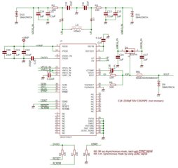
Following the notes reported inside the DAC8771 (SLASEE2 - Feb 2018) on page 66 I think that the right config is the one show into the Figure 130 where the VNEG_IN is tied to 0V, I'm right?

If this is the proper connection I think also that I've to disable the negative leg of the Buck-Boost because not used due to unipolar output type (4-20mA) so into the register 0x07 I've to use PNSEL[1.=]=01, right?

Regarding the protection TVS on the VPOS_IN, from the DAC8771EVM schematic there is a resistor named R2 (10R 0603) the purpose of this is to limit the current inside the output capacitor C1 to limit the voltage drop in the event of a voltage spike from the output?

Thanks and best regards.

F.

  • Hi,


    You are correct in the setup of the DAC8771 for disabling the negative leg of the buck-boost shown in Figure 130. The VNEG_IN is tied to 0V and you would set PNSEL to 01 to enable the positive arm but disable the negative arm of the buck-boost.

    As a warning, I've recently tried this setup when VNEG_IN is not equal to 0V and I've had the power consumption go unexpectedly high. I'm not sure if this is a problem in the setup, or rather that the device isn't meant to have an external negative supply (as opposed to ground). At this point, I would certainly test your own case (with the VNEG_IN equal to ground) with the EVM. I will try to do the same, but I believe that using VNEG_IN as ground should be a valid use case.

    The R2 of 10Ω on the EVM with C3 and C5 act as a snubber circuit for the buck-boost. This can help reduce over-voltage spikes in the switching.


    Joseph Wu

  • Thanks Joseph,

    about the VNEG_IN tied to 0V kindly let me know if this is a valid solution without trouble or is better use VNEG_IN regarding the fact that the output is only unipolar (in my case a 4-20mA current output).

    Actually I've a very little board (49mm in diameter), 4-layers, here a screenshoot:

    so I've to carefully evaluate if I've to mount all the buck-boost components or simply tied the VNEG_IN to 0V, I've put all the components, so in either situation I'm able to properly configure the board.

    About the implemented schematic regarding the DAC section here below a detail, I can use C13, C15 as 0R if I've to short VNEG_IN to ground.

    Thanks in advance for your time in testing this solution with the EVM, I'll wait for your appreciated feedback upon this point.

    Best regards.

    F.

  • Hi,

    Sorry, but I didn't get a chance to use the EVM to look at this yesterday. I should be able to get to this later today.

    Joseph Wu

  • Ok thanks, just let me know so I can step further with the PCB building.

    Thanks for yout time!

    Best regards

    F.

  • Hi,

    I've taken a quick look at the EVM and I don't see any extra current draw in when the VNEG_IN is tied to ground. It draws the same amount of current in the tests that I ran for current output. When I set it in voltage output it also draws the same amount of current (although there is a large zero code error because the output buffer amplifier now has 0V as the negative supply). I think tying the VNEG_IN to ground when not using the negative buck boost should be fine.

    I think the schematic looks ok. The schematic looks like the EVM and I think the EVM works well for many applications. I would note that we are using a Wurth 74408943101 inductor on the EVM. From the datasheet, the recommended value for the external inductor is 100 µH with at least 500 mA peak inductor current. Peak inductor current should be rated at 500 mA or greater with 20% inductance tolerance at peak current. I'm not sure what you are using, but you will want to follow this recommendation.

    Joseph Wu

  • Thanks Joseph for your great support!

    Best regards.

    F.

  • Dear Joseph,

    another things regarding the DAC8771RGZT, if we use a microcontroller powerd at 3.3V can we able to driver properly the input pins of the DAC with particular reference to the SDIN, SDO, SCLK, /SYNC pins?

    I think is possible from datasheet point 7.3

    Thanks and best regards.

    Fabio

  • Fabio,

    From the datasheet, it looks like the microcontroller should be able to send data even with the supply being run at 3.3V. The DAC8775 VIL value is 2V minimum, and I would imagine that the microcontroller output would be able support that.

    However, can the microcontroller tolerate the digital output from the DAC8775? The digital output high voltage would likely be at 5V. I don't know what the SDO maximum current is, but I would be concerned that it might damage the microcontroller.

    Joseph Wu 

  • Thanks Joseph,

    from the microcontroller datasheet a PIC16LF18446 I can see that

    then if the output voltage from the DAC digital pins is up to 5V the microcontroller will get damaged so if I need to use this model I've to add a resistor divider or a limiting resistor current into the input protection diodes or better choose the version that can be powered at 5V supply voltage.

    Thanks and best regards.

    Fabio

  • Fabio,

    It's good that you noticed that. While resistors may help, I think digital level shifters would be useful for this application.

    Joseph Wu