Good day,TI expert,
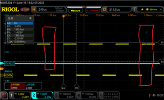
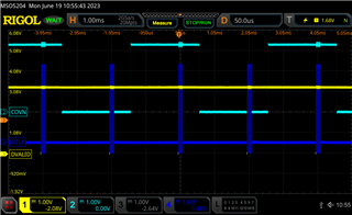
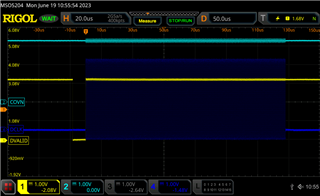
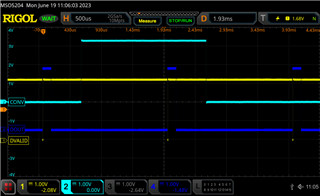
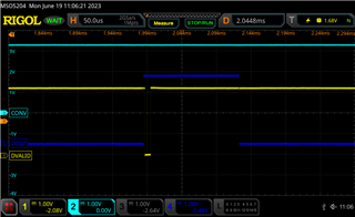
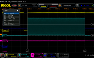
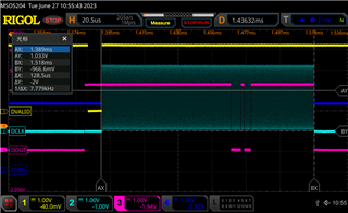
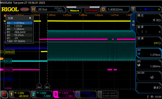
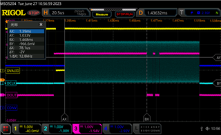
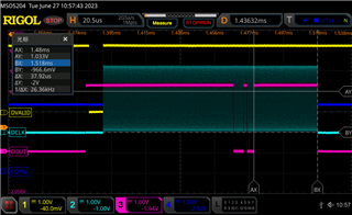
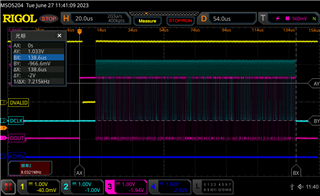
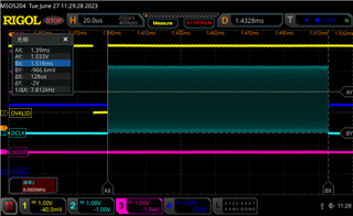
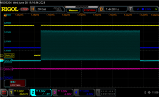
I found the DAVLID goes active high not low and it not goes active after CONV toggled all the time.
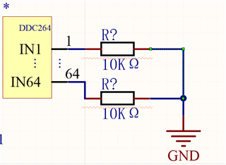
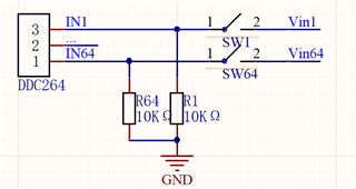
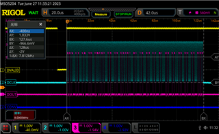
I have connneted the analog input pin in series with 10KΩ resistor and GND,as follow:
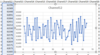
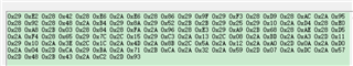
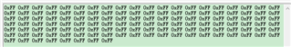
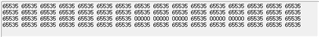
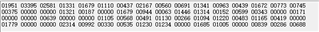
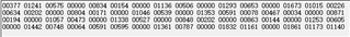
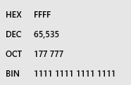
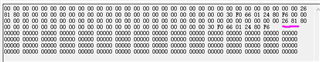
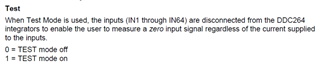
but I recevie random data in "test mode off".
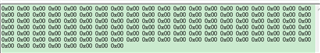
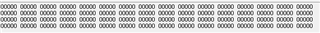
all zero in "test mode on".
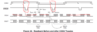
I just act DCLK after DAVLID move when my customer send command to take the data.
Is it the problem?
If not,what would make DAVLID output abnormal?
Thanks for your reply.


 .
. ,
,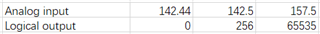
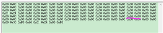
 output zero.