


Other Parts Discussed in Thread: ADS1298
Hello,
iam trying to establish a communication from STM32F4 (MASTER) to ADS1298(SLAVE). In the SPI configurations ,
SPI Mode : Clock polarity :1and clock phase :1
Full duplex master
the pin configuration of spi in stm32 and ads1298
from the MMBO BOARD to the ads1298 front end for power
J5.5---------j4.5
j5.7---------j4.7
j5.9--------j4.9
j5.10------j4.10
now, from stm32f4 to ads1298
stm32 ads1298
cs--------------------------j3.7
sclk-----------------------j3.3
mosi---------------------j3.13
miso--------------------j3.11
drdy-------------------j3.15
gnd---------------------j3.4
start-------------------j3.14
reset------------------j3.8
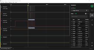
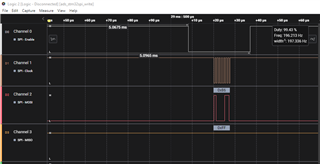
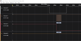
in the config1 register of ads1298, iam trying to write the value 0x86 . iam using the opcodes to write the value to the register. So in the logic analyzer, we are able to see the mosi lines , but miso lines are showing 0xFF.Iam herewith attaching the logic analyzer snapshot for the reference. while checking the power up sequence, the VCAP is showing 0v. i humbly request for a proper solution.