This thread has been locked.

If you have a related question, please click the "Ask a related question" button in the top right corner. The newly created question will be automatically linked to this question.

ADS114S06: RF sensitivity to conducted immunity test

Part Number: ADS114S06
Other Parts Discussed in Thread: DAC161S997

We've been testing a product that uses this ADC to convert a mV pressure transducer signal to 4-20mA output current with the DAC161S997 and a microcontroller.

When we apply a IEC 61000-4-6 test with 3V p-p 80% AM common-mode RF interference (0.15-80 MHz) with a EM clamp injection to the loop wiring (unshielded twisted pair), I get a quite significant DC offset shift in the ADC output at certain frequencies.

The EM clamp is on the portion of loop wiring with one conductor going to the positive terminal of the 24VDC power supply and the other conductor going to a Fluke loop calibrator and through it, back to the negative terminal of the power supply.


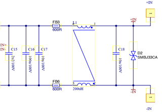
The loop wiring before the DAC161 and the 3.3V linear regulator has the following filters

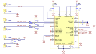
and we are using the ADC in the following way

We've tried with several variations of removing the CM choke, changing the ADC bridge input filters, and so on, but nothing seems to help for this particular product.

I would greatly appreciate any help anyone can offer as I'm mostly out of ideas at this point.

  • Hi Gaurav Hirlekar,

    Passing IEC tests is not a trivial task.  You have not stated how much shift you are seeing and what inputs are be converted as the testing is taking place.  A DC shift can take place if the analog inputs are picking up the RFI.  I don't see any additional filtering on AIN4 input.  If the 3.3V supply shifts slightly, there can also be a DC shift on the analog conversion either by reference shift or the AVDD supply itself.

    PCB layout can also play a factor as well as component placement.  It would be helpful to know the ADC configuration register settings.  Generally we don't recommend placing ferrites on the analog supply as this can sometimes be a larger problem overall as the ADC demands current.  If the ferrite is loading RFI this could be an issue with a droop on AVDD.  You might consider using a low-pass filter instead by replacing the AVDD ferrite with a small value resistor (1-10 Ohms).

    Best regards,

    Bob B

  • Dear Bob,

    AIN2-AIN3 is connected to a resistive bridge with a full span of 50mV when fed by 3.3V input excitation. I am seeing an ~3-4 mV input offset shift which is 6-7% of the total input span. The device accuracy class is 0.1% so needless to say, I am quite far from achieving it. This channel is read continuously with the following register configuration
    MUX -> AIN2-AIN3
    PGA -> enabled, gain 32
    MODE -> continuous, 200sps, LL filter
    REF -> external REFP0-REFN0 selected

    AIN4 is connected to a temperature diode which is fed 250uA by IDAC1 which causes ~0.6V drop across it. It is read once every 5 seconds with the following configuration
    MUX -> AIN4, AINCOM
    PGA -> enabled, gain 1
    MODE -> single, 2000sps, LL filter
    REF -> internal 2.5V enabled and selected

    Until now, I had not added any filtering to the AIN4 channel as I felt it is a low impedance source which would not pick up weak RF signals. Would you recommend I filter that too?

    The bridge excitation and ADC reference is derived from the 3.3V supply through a ferrite, and as the ADC input is read ratiometrically to it, so I had expected that any shift/droop in the supply would not make a difference. I guess this may not be the case. In another design, I had fed the bridge from the REFOUT pin of the internal reference, expecting it to be much more stable than the supply voltage. We had much lesser input offset shift on that board (~0.6mV) but that was an entirely different design, so I cannot be sure that this excitation method was a big part of the reason for the results.

    Is PCB layout as critical for conducted interference as it is for radiated? The entire circuit is on a 25mm round PCB with the loop side circuits on top side and the ADC on the bottom side, and the individual traces are less than 10mm long. Aren't those too small to pick up the frequencies at which we are seeing RFI issues? My team is not too experienced with EMC yet, so I could be way off the mark here.

    Until now, I had expected that the ferrites would block out the RFI due to their high impedence at those frequencies, rather than load the RFI and cause any droop on AVDD.
    I can try replacing them by 10 ohm resistors. Would you also recommend the same for FB7 which filters the bridge exitation voltage from the 3.3V supply?

    Best regards,
    Gaurav.

  • Hi Gaurav,

    It is very difficult to recommend what to do as you are very familiar with your design as to where I am not.

    Until now, I had not added any filtering to the AIN4 channel as I felt it is a low impedance source which would not pick up weak RF signals. Would you recommend I filter that too?

    As it has not yet been defined how the RFI is affecting the system, a lowpass filter may be beneficial to prevent/limit aliasing.

    The bridge excitation and ADC reference is derived from the 3.3V supply through a ferrite, and as the ADC input is read ratiometrically to it, so I had expected that any shift/droop in the supply would not make a difference. I guess this may not be the case. In another design, I had fed the bridge from the REFOUT pin of the internal reference, expecting it to be much more stable than the supply voltage. We had much lesser input offset shift on that board (~0.6mV) but that was an entirely different design, so I cannot be sure that this excitation method was a big part of the reason for the results.

    The measurement is ratiometric with respect to variations in the supply (drift).  However, interfering signals may change the ratio due to differences in filtering.

    Is PCB layout as critical for conducted interference as it is for radiated?

    Yes, maybe even more so as signal levels are so small and you are gaining them up.  The analog input should have a solid ground layer under the input signal traces and ADC.  Again, as we do not know exactly how the RFI is getting into the ADC, it is difficult to make additional recommendations.

    Best regards,

    Bob B

  • Dear Bob,

    I guess I’ll just have to try different variants and just see what works with experimentation.

    Thanks for your help.

    Regards,
    Gaurav

  • Hi Gaurav,

    One method to resolution is a shot-gun approach by just changing devices and combinations until you get things working.  Another way is to follow a logical plan of discovery at to how the RFI is getting into system aside from the EM clamp.  If it is solely coming from the loop wiring, maybe a different twist of wires is a fix.

    If the RF is escaping the loop wiring (maybe at the attach point to the PCB) then anything connected to the analog inputs could be affected.  If the bridge measurement has exposed wiring, then this too could be a pickup issue.  Maybe adding some ferrites in series with the input filter resistors can help limit the RFI from getting to the ADC inputs.

    You may also need to add some filtering to the external reference input as currently you only have a differential capacitor.

    TI does a fair amount of IEC testing as well, so I know that it is not a trivial task to pass or troubleshoot a system design.  This becomes even  more problematic when the testing is at a remote lab as often you cannot probe around the board with an oscilloscope.  For basic tests I use an inexpensive walkie-talkie to emit RF near what I would deem sensitive locations to try to pinpoint what might be happening to fix appropriately.  This has limited the amount of guess work and experimentation to see if the issue is resolved.

    Best regards,

    Bob B 

  • Dear Bob,

    if the walkie-talkie has different frequencies than the actual test equipment, would it still work?

    You are right the bridge does have exposed wiring. Perhaps I should first try adding ferrite beads to the ADC input to stop any RF pick up there.

    The entire circuit and bridge sensor and wiring is closely enclosed in a metallic enclosure. Initially, I had assumed that this would help in keeping external RF fields outside, but perhaps the RF is leaking to the metallic enclosure from the loop wiring once it enters the metallic enclosure and getting coupled to the bridge wires that way.

    Regards,
    Gaurav

  • Hi Gaurav,

    Even though the walkie-talkie has potentially different frequencies of interest, it is very helpful in helping to find the most sensitive areas of the design.

    Best regards,

    Bob B