This thread has been locked.

If you have a related question, please click the "Ask a related question" button in the top right corner. The newly created question will be automatically linked to this question.

ADC12DJ5200RFEVM: ADC12DJ5200 EVAL board: LMX2594 Device inteface with FPGA

Part Number: ADC12DJ5200RFEVM
Other Parts Discussed in Thread: LMX2594, SN74LVC8T245, TXV0108-Q1, SN74LV4T125, SN74LV1T126

Hi,

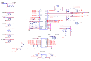
In ADC12DJ5200 EVAL board LMX2594 device inputs like CS, SCLK, SDI signals coming from FPGA are level translated to 3V3 from 1.9V using SN74AVC4T774RSVR device and outputs from level tranlator are connected to FET Multiplexer. I have query on the 3V3 level tranlation.

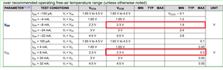
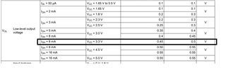
For Level translator IC SN74AVC4T774RSVR Output voltage levels at 3.3V are VOH level is 2.3V and VOL level is 0.7Max, whereas LMX2594 device input logic levels are VIH level is 1.4V and VIL level is 0.4 Max.

How both devices are compatible with each other, level translator VOL is higher than the VIL level of LMX2594 Device.

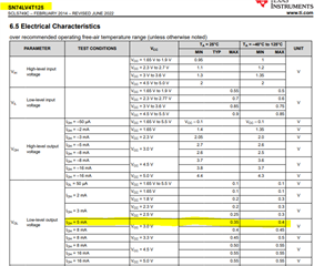
In my case, my FPGA will support only 1.8V level whereas LMX will support 1.8V to 3V3. If I want to connect CS, SCLK, SDI signals directly from FPGA then VOL(max) is higher than LMX VIL (max). I have to convert 1.8V levels to 3.3V, in this case almost all the level translators output logic level at 3.3V is VOH level is 2.3V and VOL level is 0.7Max.  which will create issue for 3.3V level

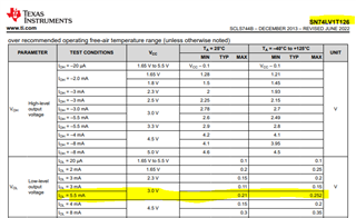
So, Instead of converting it to 3.3V Iam converting it to 2.2V so that Output level of level translator will match to the LMX2594 device inputs.

Please find the below given image for the same.

I want to know that in eval board how that logic working?

Do we need to really do the level translation for this issue, or from FPGA directly can we connect all LMX2594 devices?

Please clarify.

  • For the LMX2594, we need the signal to be low 0.4 V to be ensured it is low and above 1.4 V to be ensured it is high.  There might be some margin, but pushing 0.4 to 0.7 is pretty far off, so not the kind of thing i would try in production.

    Now if you were to take a signal that was 2.3 V min and 0.7 V max and use a resistive divider to multiply by a factor of 1/3, like series 10k and shunt 22 k, then this should get you in range.

    Now for this IC SN74AVC4T774RSVR, it sounds like it might be creating an unnecessary science experiment.  If you have 1.9 V logic, then as long as your high is above 1.4 V and your low is 0.4 V or less, it should work with direct connection.

    Regards,
    Dean

  • Hello Dean,

    Thank you for your response.

    At FPGA I have 1.8V Logic, whereas VOL Max of FPGA is 0.45 and LMX2594 VIL Max is of 0.4V.

    In this case also Can I directly connect signals from FPGA?

    Please review attached image for LMX2594 Design and provide your feedbacks?

  • Harshitha,

    High:    1.8 V > 1.4 V ?   OK

    Low:    0.45 < 0.4 ?, No, not meet spec

    You are putting 0.45 V when our spec is 0.4 V.

    As the spec is 0.4 V, I cannot say that it will certainly work with 0.45 V.   I think that this will probably work as this is only 0.5 V push for both the parts combined, but I cannot guantee this would work.  So technically to be within specification, you would need some sort of level translator or voltage divider.

    Regards,

    Dean

  • Hi Harshitha,

    almost all the level translators output logic level at 3.3V is VOH level is 2.3V and VOL level is 0.7Max.  which will create issue for 3.3V level

    Note the VIH for the LMX device seems to be 1.4V min and up to Vcc. Hence, 2.3V should be fine.

    Your schematic also seems to show SN74LVC8T245. You may also see TXV0108-Q1 for a lower VOL translator, thanks.

    Best Regards,

    Michael.

  • Hi Michael,

    Thank you for your response.

    In my schematic Iam using level translator to convert voltages from 1.8V To 2.2V, so as per the level translator datasheet VOL Max at 2.3V is 0.3V which will resolve Lower VOL level also. Can you please check and confirm us whether can we use 2.2V?

    I have one more query on the muxout signal level translator.

    For LMK_MUXOUT  we are using saperate level translator to convert from 3.3V to 1.8V, and for other SPI lines I am using different level translator (refer the attached schematic). Will it cause any timing issues for SPI interface (muxout)?

  • Hi,

    Awaiting for your response

  • Hi Harshitha,

    Are you asking about the level shifter or the LMX?

    Please note that, no concerns for the level shifters, thanks.

    Best Regards,

    Michael.

  • Hi Micheal,

    thank you for the response.

    So, can I use different Level shifters for MUXOut and for SPI LMX2594 input signals?

    Please review the below image.

  • Hi Harshitha,

    Yes you can. For example, you may also see SN74LV1T126 with lower VOL for the MUXout and SN74LV4T125 for the SPI inputs.

    Also note that the specified values in the datasheets are at maximum for the IOL driver and customers cases would most likely be less, thanks.

    Best Regards,

    Michael.

  • Hello Micheal,

    Thank you for the response.

    In LMX2594 Device data sheet VIL Max is mentioned as 0.4V wheras in level translator Datasheet @3V it is mentioned VOL Max as 0.7V.

    In this case VOL is greater than VIL, If I connect both devices will it be compatible with each other? For Logic "0", voltage levels are not in valid range. Please check and confirm the same.

  • Hi Harshitha,

    Which level translator datasheet is being referred to? Would it be feasible to consider the recommendations shown below?

    Best Regards,

    Michael.

  • Dear Micheal,

    I was referring to SN74LVC8T245 this IC Datasheet.

    I looked into sn74lv4t125 device datasheet, In this device also I have a concern for Logic "0" voltage level. As per the below image for VCC=3V3 then VOL max is 0.45 (25Deg) and 0.5V (High temp) and LMX2594 device VIL Max is 0.4V. For logic 0 level it will cause an issue. Please check and confirm?


  • Hi Harshitha,

    Note that the maximum is worst case maximum across process variations, voltages, temperatures and would most likely not be observed for your system.

    For the LVC8T device for example, I got some bench data yesterday and observed about 0.1V typical low voltage on the output for 1.8V to 3.3V as shown below (C2 as the input, C3 and C4 both as outputs with different probes/load).

    Hence, I would recommend verifying per your system requirement for your device of interest and the 0.4V requirement should not be a concern, thanks.

    Best Regards,

    Michael.