This thread has been locked.

If you have a related question, please click the "Ask a related question" button in the top right corner. The newly created question will be automatically linked to this question.

AFE58JD48EVM: Ramp pattern test for LVDS

Part Number: AFE58JD48EVM

Hi, we have 2 questions about the EVM:


1) We are using the EVM board's GUI to configure the ADC chip, and for initial testing, we also use the internal ramp generator( default setting for its data format ) to test the LVDS I/F going to an FPGA EVM. The datasheet doesn't mention the data format of the generator. Is it unsigned or 2s complement ? If the output format can be configured, we'd like to know how.


2) Once all GUI configuration steps are done, we want to change the clock from using 40MHz ( confirmed ) to prescale it down to 20 MHz. Is the prescaler in register 0x29 and are there any other registers to be changed to make the new setting take effect ?

  • Hi Jerome,

    Thanks for reaching out.

    Please find my comments inline.

    1) We are using the EVM board's GUI to configure the ADC chip, and for initial testing, we also use the internal ramp generator( default setting for its data format ) to test the LVDS I/F going to an FPGA EVM. The datasheet doesn't mention the data format of the generator. Is it unsigned or 2s complement ? If the output format can be configured, we'd like to know how.

    TI: The default data format is 2s complement.

    2) Once all GUI configuration steps are done, we want to change the clock from using 40MHz ( confirmed ) to prescale it down to 20 MHz. Is the prescaler in register 0x29 and are there any other registers to be changed to make the new setting take effect ?
    TI: I could not follow your question. Are you looking to reduce the adc input clock to 20MHz (In that case you can use external clock input on the EVM and provide 20M clock)

    We don't have any prescalar to divide the clock by 2.

    Thanks & regards,

    Abhishek

  • Hi Abhishek,

    The info is appreciated !

    1) So, just checking that the ramp generator data output cannot then be changed to unsigned and can only output in 2s complement ? I assume the ramp starts at zero, and so doesn't go thru any (-)values ?

    2) I shouldn't have mentioned register 0x29 ( register in the ADC ), but I meant prescaler on the LMK clock chip. I should be able to use  the GUI to adjust the prescaler of the LMK ?

    Regards,

    Jerome

  • Hi Jerome,

    1) So, just checking that the ramp generator data output cannot then be changed to unsigned and can only output in 2s complement ? I assume the ramp starts at zero, and so doesn't go thru any (-)values ? 

    TI: The output format is 2C hence you need to treat the data as 2C and plot.

    2) I shouldn't have mentioned register 0x29 ( register in the ADC ), but I meant prescaler on the LMK clock chip. I should be able to use  the GUI to adjust the prescaler of the LMK ?

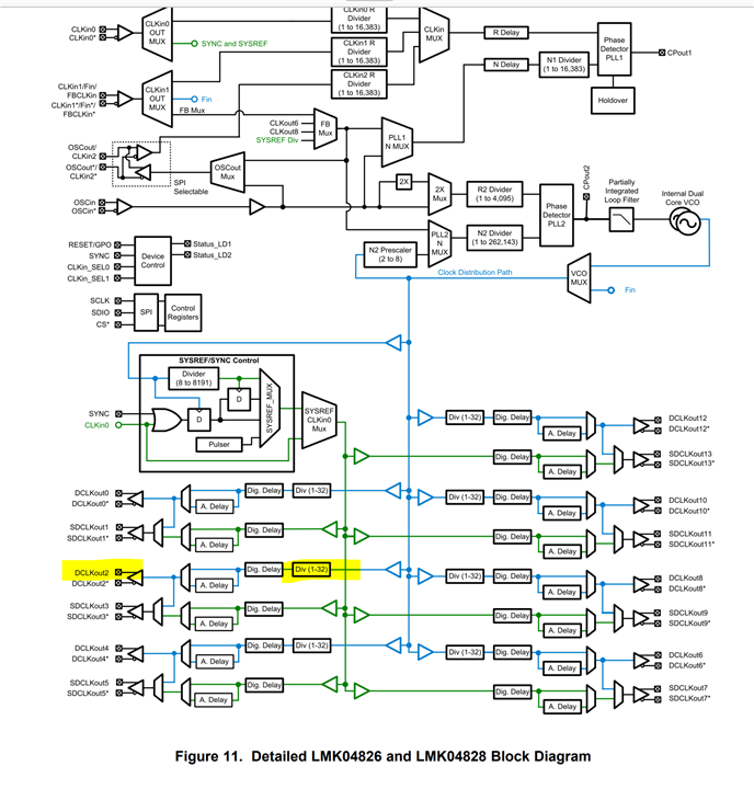
    TI: Yes, you can configure the LMK in clock divider mode (CDM) and just use the final divider to set the ADC clock. Figure below shows the corresponding block I am talking about. Highlighted in yellow is the divider. The corresponding SPI address for the divider is also shown below.

    Thanks & regards,

    Abhishek