This thread has been locked.

If you have a related question, please click the "Ask a related question" button in the top right corner. The newly created question will be automatically linked to this question.

DAC8771EVM: first testing with the EVM, DAC8771 is hot with DIG_Supply 5V and other question

Part Number: DAC8771EVM
Other Parts Discussed in Thread: DAC8771,

Dear Sir,

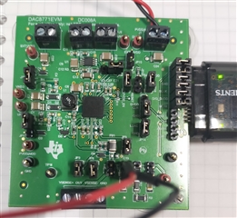
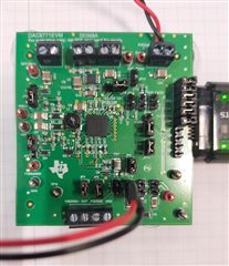
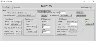
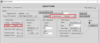
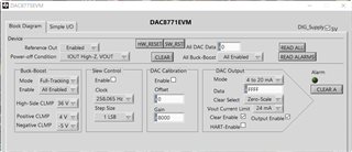
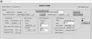
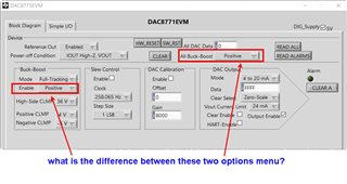
I'm doing first testing with the EVM, 12V input supply, output 4-20mA. Touching the DAC reveal that this is hot with the DIG_supply checkbox is selected (related right label report 5V), when I uncheck this box label report 3.3V and then the chip is no more hot.

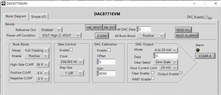
Here below my actual jumper settings:

JP1: 1-2

JP2: 1-2

JP3: installed

JP4: not installed

JP5: installed (load 249ohm)

JP6: not installed

JP7: not installed

JP8: installed

JP9: installed

JP10: not installed

JP11: 1-2

JP12: 2-3

JP13: not installed

JP14: installed

JP15: not installed

JP16: not intalled

JP17: unable to find it inside the board...

So you have some hint, note?

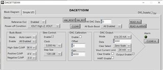
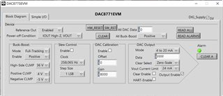
Also READ ALL active every time HART-Enable despite I've unchecked the relaterd box...

Thanks and best regards.

FF

  • Now I've installed JP15 and JP16, Alarm is always green, voltage on the TP7 DVDD test point, with the DIG_Supply unchecked give me 0.8V, while checked (DAC8771 get hot) give me no more than 1.2V like there is some short-circuit on some part.... I've to know if this due to jumper settings or is about the EVM itself...

    Kindly let me know, thanks.

    FF

  • UPDATE - WORKING BOARD

    After some test I've did the system properly working.

    I've removed the JP15 and JP16 jumper to separate the DIG_VDD line that came from the SM-USB-DIG, this prevent any short circuit between the internal LDO and the DVDD voltage output generated from the SM-USB-DIG adapter.

    Here below the final working configuration for the jumper:

    and the used working GUI settings for the 4-20mA output.

    Now I'm using the 249 ohm onboard load (JP5 is used to feed an external 6 digit 1/2 calibrated ammeter), I've measured:

    DAC Settings - measured current - absolute error (relative to the theoretical value) - percentual error

    0x0000 : 3.9646mA : -35.4 uA :

    0x4000 : 7.9268 mA : -73.2 uA

    0x8000: 11.8916 mA : -108.4 uA

    0xFFFF: 19.821 mA : -179 uA

    are reasonable without doing DAC calibration?

    DAC Calibration question

    After check the DAC Calibration box inside the GUI I've did some change at the Offset value but no change I've see into the measured current output, there are other special settings to do in order to use immediately the calibration values?

    Thanks and best regards.

    FF

  • Here the Iout Vs DAC Code diagram, there is also the percentage error measured, this diagram is substantially the same over all the VIN span between 12V and 24V.

    The maximum percentage error between the output measured current and the theoretical one was equal to -0.926%

    Thanks and best regards.

    FF

  • FF,


    First, I'm glad you were able to get the device working. As you had mentioned, JP15 and JP16 should separate the internal LDO from the external DVDD driver from the SM-USB-DIG. It can be set up with the DVDD driven from the SM-USB-DIG, but the DVDD from the device must be disabled through JP15.

    For your plot, the only thing that I see that is wrong is that I think the error for the first point should be negative. The numbers that you show in the previous post shows the 0x0000 value of 3.9646mA is a negative error, similar to the negative errors in all the other points.

    The error of approximately 0.926% seems a little high. However, you may not have accounted for the reference error. For the device, we separate the error of the DAC from the error from the reference. When making this measurement, also take the measurement of the reference voltage to eliminate that error.

    Regardless, the next time you take this data, you can include all of the measurement values in an excel spreadsheet, and I can look over the data.


    Joseph Wu

  • Dear Joseph,

    thanks for your prompt reply!

    Here the measured value in Excel.

    The error are all negative, the error is reported on the secondary axis at the right side of the diagram.

    Thanks and best regards.

    FF

    DAC-measured-value.xlsx

  • Dear Joseph,

    I see another strange behavior, with 1k load (so JP7) I'm unable to reach the 20mA output current despite the VIN is up to 30V, the positive boost voltage is equal to 20.835V and the 0x0B register value is equal to 0x1781, the alarm action register 0x0D report a value of 0.

    Do you have some suggest?

    If I I change the Busk-Boost settings as into the image below:

    the VPOS of the Buck-Bost increase up to 22.223V (Vin 24V-30V is the same), output voltage on TP3 is equal to 19.376V and the measured current is only 19.325mA, from this test seems that the module is not able to work properly at the 1k ohm load... do you have some hint about that?

    Thanks and best regards.

    FF

  • FF,

    I'm not sure what the problem is with that. I would try setting the Mode to Clamp, and then setting the Positive CLMP to 30V. Then check the VPOS_IN and the output voltage. It normally should easily track to 24mA with a 1kΩ load without user adjustment, so I'm not sure what is going on.

    Joseph Wu

  • FF,

    Also, I looked at your excel data, and I looked at an end point non linearity, and there is some non-linearity that I can see. I'm not sure where it comes from, but it seems to be largest at the 0000 DAC code point. I would look at a few more points near the 0 code. Attached is the excel file that I altered to add in some INL calculation columns.

    Because this is a current output DAC, I wouldn't expect any zero code error. Again, I would also measure the reference value along with the output measurements. 

    Joseph Wu

  • I forgot the file:

    DAC-measured-value2.xlsx

    Joseph Wu

  • Hi Joseph,

    here the Excel file with more measurement around 4mA, let me know if you need other ones or other measurements. I've also put the GUI settings used to perform these measurements.

    I've did it only for VIN=24V that will be my working voltage (so I've removed the VIN=12V worksheet).

    Thanks for your time!

    FF

    1263.DAC-measured-value2-only-VIN-24V.xlsx

  • FF,


    For the DAC output with a 1kΩ load (at 20mA output), I was able to get the full output of the DAC with one change of setting. The Power-off Condition (under the Reference Out setting) must be set to IOUT High-Z, VOUT High-Z. This is changed from IOUT High-Z, VOUT 30kOhms.

    If the device is set to the latter setting, I get results similar to you where the IOUT=19.3mA with VPOS=22.1V.

    If the device is set to the former setting, I get IOUT=19.97mA where VPOS=22.8V.

    Again, the Power-off Condition should be set to IOUT High-Z nd VOUT High-Z. This should get you the full output range.

    Joseph Wu

  • Dear Joseph,

    thanks for your time.

    Concering the test at 1k load, I've also to set the Buck-Boost enable option to Positive, if I use the All Enable option the maximum output current is limited to 19.19mA, hence with only the option Positive I've 19.9929mA on a 1k load, VPOS=22.867V.

    Here below my working GUI settings.

    Could you please check on your side?

    Here the Excel file with the measured value at these operative conditions.

    DAC-measured-value2-only-VIN-24V-RL-1000.xlsx

    Also I've a question around the GUI interface, what is the difference between the All Buck-Boost drop down menu into the Device section regarding the Enable drop down menù into the Buck-Boost section?

    There is a way to get the whole registers value in a single file directly from the GUI form or the only way is read registers one by one through the Simple I/O panel? This will be useful in order to have all the relevant registers value when I've to program my custom board that is equipped with a microcontroller.

    Thanks and best regards.

    FF

  • Another question that I've noticed is about alarm settings.

    Check this condition (VIN=24V, RL=1k, Buck-Bosst enabled only the positive section):

    in this situation the output current measured is equal to 3.998XX mA (the last XX digit is changing between 43 and 54).

    Now set the maximum value so 0xFFFF, the output current value change accordling to 19.9930mA, but if I went to perform a read alarms I'll see that the Alarm led is set

    then through the Simple I/O panels reading of the 0xB register (STATUS) give the value 0x1781 so DAC Fault (F) bit is set.

    Now the question is why the system show this fault flag activated?

    Going back to main form by clicking the Block Diagram panel on the form and then press the button CLEAR A will reset the alarm flag(s), so by pressing again READ ALARMS the Alarm led is found set to the inactive state.

    This behaviour is only with 0x0000 to 0xFFFF transition, so I've tried to set the Slew Control as shown below:

    and now seems the the Alarm is not be triggered when the 0 to 0xFFFF transition is set.

    Could you please also perform a similar check at your side?

    Thanks and best regards.

    FF

  • Dear Joseph,

    I've did registers reading through the Simple I/O panel and using the Read Register section, but seems to me that not all the register are read properly, for example reading the 0x04 register give me always 0...

    there is some trouble with this function on the GUI?

    Thanks and best regards

    FF

  • FF,


    Yes, the alarm will go off if you set the device to transition from the lowest value to full scale under the default condition of the DAC. The alarm is set depending on several conditions described on page 37 of the datasheet. One of the conditions is when the voltage at IOUT reaches a level where the accuracy of the output is compromised for greater than 500us.

    For the way that you have the device set up, this condition is reached because the VPOS_IN is set low, and it must track up as the IOUT is set to the highest value. If you are using the 0-20mA range, when IOUT is 0mA, VPOS_IN is about 4V as the default. If the DAC is set to 20mA, the output will track out to 20V with a 1kΩ load. However, the VPOS_IN starts out as 4V and it takes time to ramp so that it ends at 23V so that the output is set correctly. Because it takes about 1ms to set the supply, the alarm is set.

    To avoid this alarm, you can set the VPOS_IN to the proper voltage before setting the IOUT current. Set the mode to Clamp, set Positive CLMP to 23V, and then set the IOUT from 0000 to FFFF. In this condition, the device does not have a time period where the IOUT voltage is compromised.


    Joseph Wu

  • FF,

    Also, I generally don't have any issues reading the device. Have you tried reading the other registers? I would note that the 0x04 register is 0 for default. 

    Is there any particular sequence of communication that you've sent that gives you the 0 reading?

    Joseph Wu

  • I've reloaded the GUI, now the register value looks properly.

    Thanks for the info about the Alarm on transition between 0 and full scale! Well, in my application this condition will never occour then was just for my extensive testing of the chip that I've noticed this behaviour...

    Best regards

    FF

  • Dear Joseph,

    I'm working around the SPI in order to drive the DAC8771EVM from J1 connector using MISO, MOSI, SCLK, SYNC, GND lines from a microcontroller evaluation board. The microcontroller is powered at 5V, of course I've detached the SM-USB-DIG adapter from J2 before attaching the microcontroller board.

    I kindly ask what is exactly the SPI mode supported? The DAC8771 on what clock edge will sample the incoming data on the MOSI line?

    Looking at the Figure 1 on the datasheet from t7 and t8 I can suppose that the data is sampled inside the DAC8771 on the falling edge of the clock and shifted out on the rising edge so mode 1, I'm right?

    Thanks and best regards.

    FF

  • FF,

    It looks like you have things working for the most part. One thing that I wanted to remind you is that the Power-off Condition setting with IOUT High-Z, VOUT 30kΩ will give you some amount of error unless you set the VOUT to High-Z. 

    For this particular board, the VOUT and IOUT are in parallel, and if you have the VOUT 30kΩ resistance set, it will still be there when just using IOUT mode.

    Joseph Wu

  • FF,

    Yes, you are correct. The DAC8771 operates with SPI such that the SCLK idles low, the data (DIN or SDO) is valid at the falling edge of SCLK.

    Joseph Wu

  • Thanks Joseph!

    I've succesfully written the DAC8771 register through the SPI interface so I was able to send commands to the DAC8771 from my microncontroller evaluation board.

    Now I've to work around the reading command, do you have some other info than the ones reported into the datasheet, it is not so clear, seems the after the writing command related the reagister that I've to read I've also to send another command (NOP so register address 0x00 with value to sent equal to 0x00) in order to read the answer from the DAC (figure 2, page 14 and page 42), to instruct the DAC8771 that is a read operation the 23bit (MSB) of the frame hence the MSB of the byte rtelated to the address, part should be set to 1. I'm right?

    UPDATE

    I've did succesfully to manage the SPI read and is working properly so now I can write and read DAC8771 registers through the SPI; now I've a question related the alarm (register 0x0B), how to perform the CLEAR alarm operation like I can do into the GUI by pressing the CLEAR button to clear the alarm signal?

    I've also another question about the behaviour of the SPI lines when the DAC8771 is not powered by the external PVDD/AVDD but the SPI lines are phisically connected to the microcontroller and this one is powered before the DAC8771, there are some current limiting on the SPI lines, are activated the protection diodes if present on these lines ecc...?

    Thanks as usual!!

    Best regards.

    FF

  • Hi Fabio,

    Joe is working on this now.

  • FF,


    The ALARM is set based on several conditions described in section 8.3.8 of the datasheet. These conditions are all continuously monitored on the device. When the ALARM occurs, the pin is pulled low and the corresponding status bit on 0x0B is set. The ALARM pin stays low until the status bit is cleared by writing a 1 to the corresponding bit. This is described in 8.3.10 in the datasheet.

    For the DAC8771 SPI lines, there aren't any series protection diodes or resistance in the device or on the EVM board. However the SM-USB-DIG controller used for the EVM does use some drivers that seem to have some inherent protection for over-voltage/over-current events. You would need to look at the SM-USB-DIG Platform User Guide:

    https://www.ti.com/lit/pdf/sbou098

    Joseph Wu

  • Thanks Joseph to have pointed me on the right paragraph, during my datasheet reading I've not noticed this point about the alarm clearing procedure.

    Actually seems all is working properly with my microcontroller and I'm able to drive and read properly the DAC8771 through the SPI interface, just for reference for other people may be useful I'll give below some details on the read and write through the SPI.

    Update mode
    In my design the !LDAC pin is tied to 0V so the mode used is the Asynchronous Mode (page 42 of DAC8771 datasheet).

    In the following pseudocode the SPI_SendByte() function just sent a byte through the SPI interface of the microcontroller, so related implementation it is related to used microcontroller.

    DAC8771 SPI READ operation
    input: uint8_t regaddr => register address
    output: uint16_t ans => readed value

    - SYNC forced LOW
    - firstbyte= 0b10000000 | regaddr; // Set the R/W bit at 1 (datasheet page 42, Table 2)
    -  SPI_SendByte(firstbyte);
    -  SPI_SendByte(0x00);  // Payload set to 0
    -  SPI_SendByte(0x00);  // Payload set to 0
    - SYNC forced HIGH
    - delay(I used 1.75us, just check that is greater than t6 page 13)
    - SYNC forced LOW
    - SPI_SendByte(0x00); // Transmissione of NOP command (reg 0x00, payload 0x00)
    - hibyte=SPI_SendByte(0x00); // HI BYTE
    - lobyte=SPI_SendByte(0x00); // LO BYTE
    - SYNC forced HIGH
    - ans= (((uint16_t)hibyte)<<8) | ((uint16_t) lobyte); // Build the final value

    DAC8771 SPI WRITE sequence
    input: uint8_t regaddr => register address
    input: uint16_t val => 16 bit data (payload to deliver at the DAC8771)
    output: void

    - SYNC forced LOW
    - firstbyte = regaddr;
    - databytehi = (uint8_t)((val >> 8) & 0x00FF);
    - databytelo = (uint8_t) (val & 0x00FF);
    - SPI_SendByte(firstbyte);
    - SPI_SendByte(databytehi);
    - SPI_SendByte(databytelo);
    - SYNC forced HIGH

    Hope these info will be useful for other.

    Best regards.

    FF

  • FF,

    I hope this device fits your application! If you have any other questions, feel free to post back.

    Joseph Wu

  • Thanks Joseph,
    I'll step further with the development, you help me a lot.

    Best regards!

    FF