Hi,
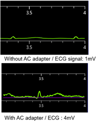
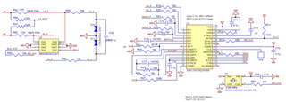
We are experiencing ECG signal interference problems and provide the register settings and circuit diagrams.
Please give us suggestions, thank you.
Register mapping,
{ 0x01, 0x0A }, // 0, 0x01,0x00; ch1-Routing;
{ 0x02, 0x1C }, // 1, 0x02,0x00; ch2-Routing;
{ 0x03, 0x2E }, // 2, 0x03,0x00; ch3-Routing; Positive:IN5 + Negative:IN6,<- A; 00-10 1-110
{ 0x04, 0x00 }, // 3, 0x04,0x00; pace-Routing; Non-Pace Channel
{ 0x05, 0x00 }, // 4, 0x05,0x00; Batt.-Routing; Non-Battery Monitoring
{ 0x06, 0x08 }, // 5, 0x06,0x08; Lead-Off Detect Control; DC lead-off detection;
{ 0x07, 0x00 }, // 6, 0x07,0x00; Lead-Off Detect Enable; 0/1:Dis/En-able Lead-Off Detect; 0x070B
{ 0x08, 0x00 }, // 7, 0x08,0x00; Lead-Off Detect Current; 25 * 0.008uA = 200nA; 0x0832
{ 0x09, 0x00 }, // 8, 0x09,0x00; AC Lead-Off Detect Control; Input signal freq.
{ 0x0A, 0x03 }, // 9, 0x0A,0x00; Common-Mode Detect Enable; Disable "Common-Mode Detect" using XX channel; 0x0A30;
{ 0x0B, 0x00 }, // A, 0x0B,0x00; Common-Mode Detect Control; Low-bandwidth mode & Medium low cap-drive mode
{ 0x0C, 0x40 }, // B, 0x0C,0x00; Right-Leg Drive Control;
{ 0x0D, 0x00 }, // C, 0x0D,0x00; Wilson Reference Input one Selection; First buffer amplifier connected to input IN1
{ 0x0E, 0x00 }, // D, 0x0E,0x00; Wilson Reference Input two Selection; second buffer amplifier connected to input IN2
{ 0x0F, 0x00 }, // E, 0x0F,0x00; Wilson Reference Input three Selection; second buffer amplifier connected to input IN3
{ 0x10, 0x00 }, // F, 0x10,0x00; Wilson Reference Control; Goldberger reference disabled & Wilson reference output internally connected to IN6
{ 0x11, 0x00 }, // 0, 0x11,0x00; Internal Reference Voltage Control; CM and RLD reference voltage is on & Internal reference voltage is on
{ 0x12, 0x04 }, // 1, 0x12,0x00; Clock Source and Output Clock Control; Start the clock & Clock to digital disabled & : Use external crystal on XTAL
{ 0x13, 0x07 }, // 2, 0x13,0x00; Analog Front End Frequency and Resolution; Clock frequency 102400 Hz & High-resolution mode
{ 0x14, 0x00 }, // 3, 0x14,0x00; Analog Front End Shutdown Control; Active sigma-delta modulator & instrumentation amplifier
{ 0x15, 0x07 }, // 4, 0x15,0x00; Analog Front End Fault Detection Control; Disable the instrumentation amplifier fault detection
{ 0x16, 0x00 }, // 5, 0x16,0x00; RESERVED;
{ 0x17, 0x01 }, // 6, 0x17,0x01; Analog Pace Channel Output Routing Control; Analog pace channel output disconnected & shut down
{ 0x1F, 0x03 }, // 7, 0x1F, Digital Output Drive Strength; Digital Output Drive Strength -- High drive mode
{ 0x21, 0x08 }, // 8, 0x21, R2 Decimation Rate; 8 (default)
{ 0x22, 0x10 }, // 9,0x22, R3 Decimation Rate for Channel 1; R1=16 => 128(25Hz)/64(50Hz)/32(100Hz)/16(200Hz)/8(400Hz)/6(533Hz)/4(800Hz)
{ 0x23, 0x10 }, // A,0x23, R3 Decimation Rate for Channel 2; 200Hz
{ 0x24, 0x10 }, // B,0x24, R3 Decimation Rate for Channel 3
{ 0x25, 0x00 }, // C, 0x25, R1 Decimation Rate; R1=4
{ 0x26, 0x00 }, // D, 0x26, ECG Filter Disable; ECG filter enabled
{ 0x27, 0x08 }, // E, 0x27, Data Ready Pin Source; DRDYB pin not asserted
{ 0x28, 0x40 }, // F, 0x28, SYNCB In/Out Pin Control; Disable the SYNCB pin
{ 0x29, 0x00 }, // 0, 0x29, Optional Mask Control for DRDYB Output
{ 0x2A, 0x00 }, // 1, 0x2A, Mask Error on ALARMB Pin
{ 0x2E, 0x33 }, // 2, 0x2E, Digital Filter for Analog Alarm Signals
{ 0x2F, 0x00 } // 3, 0x2F, Configure Channel for Loop Read Back Mode; Disable data read back
Ray Yang