This thread has been locked.

If you have a related question, please click the "Ask a related question" button in the top right corner. The newly created question will be automatically linked to this question.

DAC37J84: DAC37J84

Part Number: DAC37J84

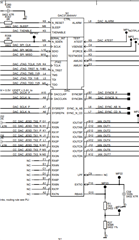
We are using the DAC37J84 as a programmable waveform generator.  The full-scale current is set up as 0.02073 A (Rbias = 1.91kOhm, course_dac = 10).  The load resistors on IOUTP and IOUTN are each 24.95 ohms.  For test purposes, the outputs are not connected to any other circuit.

When we program full-scale output, I expect 0.517 volts (0.02073 A * 24.95 ohms) on one pin and 0.000 (0.0000 A * 24.95 ohms) on the other.  We actually measure 0.594 V (15% error) and 0.077 V (infinite error).  It's as though there is an extra 3 mA flowing in both outputs.

Where does this offset come from?  Is it explained somewhere in the data sheet (SLASE17B)?  I could find no mention.

  • Hi Anthony,

    We can take a look at this. Would it be possible to forward your schematic for us to view?

    Thanks,

    Rob

  • There is a limit to what I can share, but here's the DAC showing the current output pairs and our RBIAS termination :

    And here is how each pair is terminated.  Note that for this DC testing I have removed the resistors feeding the diff-amp (R301 and R302).  With this modification each DAC current output only feeds a parallel pair of 49.9 ohm resistors.:

  • Hi Anthony,

    Thank you for the schematic captures and additional details.

    I am looking into this, if you plan to DC couple then there is probably some common mode current to accommodate for.

    The datasheet doesn't do a great job of showing how to DC couple the analog outputs. It only gives AC coupled guidance using a balun or a transformer.

    Give me a few days to respond back.

    Thanks,

    Rob

  • Hi Anthony,

    I spoke to a few people about this internally. There is an output Ibias current that is not well documented in the datasheet.

    So the expected values that you are reporting is correct.

    I am working to get you an Ibias number that you can work with, to adjust the output network for your application.

    I will try to get back to you later today.

    Thanks,

    Rob

  • Hi Anthony,

    Sorry for the delay. I am still working with production to see if they can dig up any data on the Ibias value. I did measure the DAC on the bench in the same case you outlined above and measured the same voltages. So 3mA of Ibias seems reasonable, I was just hoping to get a confirmation on this.

    Ultimately, we will need to play with the output resistor network in order to compensate for this. 

    What tends to happen here is that as the amplifier is connected to the output circuit is DC coupled, this will change the resistive network, as the amplifier will play an effect on this circuit now too.

    My assumption is that you will need to add an extra pullup resistor in your circuit in-between the output of the DAC and input of the amplifier in order to offset all the currents. This is a common DC coupling issue, where there isn't much documentation on this subject unfortunately.

    Regards,

    Rob

  • Hi Anthony,

    I apologize for the long delay.

    I finally heard back from our test engineers and they measure the output offset, which is confirmed to be 3mA.

    Regards,

    Rob

  • Rob,

    Thanks for looking into this and confirming my observation.

    Tony