This thread has been locked.

If you have a related question, please click the "Ask a related question" button in the top right corner. The newly created question will be automatically linked to this question.

ADS1248: Photodiode Sensor Used with ADC and Amplifiers

Part Number: ADS1248
Other Parts Discussed in Thread: OPA335, ADS124S08


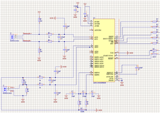
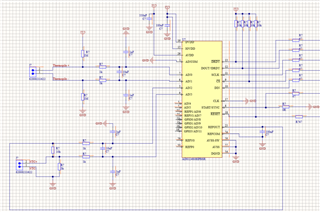
I have a photodiode sensor that gives a min-max output between 0.134 mV and 178 mV. I will amplify the output mV of this sensor using OPA335 and then give it to the ADS1248 ADC. The digital data from the ADC will be connected to the STM32F030x processor.

My questions are;

1. Are my steps correct?

2. Are the analog input-output voltages of the integrations I use suitable for each other?

3. Do I need to use another Buffer amplifier after the OPA335 Amplifier? If necessary, which one do you recommend to use?

4. How will I adjust the gain of the amplifiers and ADC I use?

Best Regards,


  • Hi Gulbahar G

    Why would you need the OPA335 if you are using the ADS1248? Can you not directly connect the output of your sensor to the ADC since the ADC has a high impedance amplifier integrated?

    Have you considered the ADS124S08? This is the next generation version of the ADS1248 that offers better performance, more features, lower power, lower noise, more channels, smaller size, and the same cost.

    -Bryan

  • Hi Bryan, 

    Thank you for your suggestions.

    In line with your suggestions, I replaced the ADS1248 ADC with ADS124S08IPBSR. I connected the thermopile and NTC resistors directly to the ADC. My schematic drawing is attached. Can you check it?

    Let's not forget that the outputs of my thermopile are in the range of 0.134 mV and 178 mV.

    How should I adjust the Gain while adjusting the PGA settings of the ADC? Can you help me with this?

  • Hi Gulbahar G,

    Some comments / questions:

    • You have a capacitor of unknown value placed between DVDD and IOVDD. That is incorrect. One pin of the cap should be connected to both DVDD and IOVDD, while the other capacitor pin should be connected to ground. You can follow the datasheet guidelines or EVM schematic for more detail about capacitor sizes, etc.
    • REFCOM needs to be grounded
    • You should probably have pull-ups on RESET and CS to make sure the ADC powers up in a known state
    • How do you plan on biasing the NTC?
    • If the resistor between REFP0 and REFN0 is connected to ground, you don't need the filtering on the node connected to ground. Therefore, you can remove the 10nF caps and remove the resistor between REFN0 and ground. Also make sure the reference buffer on REFN0 is disabled
    • Since the thermopile is biased by the pull-up / pull-down resistors, the common-mode of the thermopile signal will be centered at mid-supply, which is the desired configuration for the ADC's PGA. Therefore, you should be able to use the maximum gain allowed for your input signal range. Make sure to respect the requirements given in Equation 5 in the ADS124S08 datasheet
    • You can probably reduce the cap values on the inputs by a factor of 10x e.g. 10nF differential cap, 1nF common-mode cap

    -Bryan

  • Hi Bryan,

    I have edited my schematic drawing according to your instructions. These are the necessary arrangements, if there are other issues and details you want to suggest, I am open to the end.
    I am not sure of the pull-up resistance in the arrangements I made. Can you look specifically for it?
    Also, according to the ADS124S08 ADC datasheet equation5, gain=16 (V/V).

    Is this schematic drawing suitable for you?

  • Hi Gulbahar G

    I don't think you need pull-ups on DOUT and DRDY, unless you want to include them

    Also, I assume the 5k resistor across NTC+ and NTC- is for linearization, correct? Generally you select these components so the divider is balanced at 25C. For example, if the NTC has a nominal impedance of 10kohm at 25C, then you would put a high accuracy 10kohm resistor as the linearization resistor. At 25C, the total impedance is 10k || 10k = 5k. The bias resistor (currently the 10k resistor you have in your schematic between REFOUT and NTC+) would then also be 5k, so you would measure a voltage of 1.25 V at 25C (assuming VREF = REFOUT = 2.5V)

    Otherwise, this looks like a good start to your schematic

    -Bryan

  • Hi Bryan,

    Thank you for your attention.

    I have completed the corrections you suggested. I seem to have no other problems. I even started card design.

  • Hi Gulbahar G,

    I am glad we could help, I will consider this question resolved then

    -Bryan