This thread has been locked.

If you have a related question, please click the "Ask a related question" button in the top right corner. The newly created question will be automatically linked to this question.

ADS1298ECGFE-PDK: Getting distorted waveforms with different frequency and voltage levels

Part Number: ADS1298ECGFE-PDK
Other Parts Discussed in Thread: ADS1298,

I am currently working with the ADS1298ECGFE-PDK and have connected a waveform generator to the input pins IN2. The positive end of the waveform generator is connected to IN2P, and the ground from the waveform generator is connected to IN2N. I have configured the following registers on the ADS1298.

| Register   | Address | Value |
|------------|---------|-------|
| ID         | 0x00    | 0x92  |
| CONFIG1    | 0x01    | 0x86  |
| CONFIG2    | 0x02    | 0x10  |
| CONFIG3    | 0x03    | 0xDC  |
| LOFF       | 0x04    | 0x03  |
| CH1SET     | 0x05    | 0x91  |
| CH2SET     | 0x06    | 0x10  |
| CH3SET     | 0x07    | 0x91  |
| CH4SET     | 0x08    | 0x91  |
| CH5SET     | 0x09    | 0x91  |
| CH6SET     | 0x0A    | 0x91  |
| CH7SET     | 0x0B    | 0x91  |
| CH8SET     | 0x0C    | 0x91  |
| RLD_SENSP  | 0x0D    | 0xFF  |
| RLD_SENSN  | 0x0E    | 0x02  |
| LOFF_SENSP | 0x0F    | 0xFF  |
| LOFF_SENSN | 0x10    | 0x06  |
| LOFF_FLIP  | 0x11    | 0x00  |
| LOFF_STATP | 0x12    | 0x00  |
| LOFF_STATN | 0x13    | 0x02  |
| GPIO       | 0x14    | 0x00  |
| PACE       | 0x15    | 0x00  |
| RESP       | 0x16    | 0xF0  |
| CONFIG4    | 0x17    | 0x22  |
| WCT1       | 0x18    | 0x0A  |
| WCT2       | 0x19    | 0xE3  |


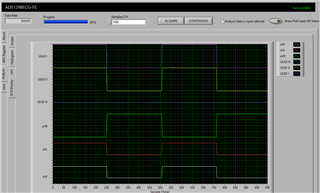
I applied sine and DC wave signals with amplitudes of 1mV, 5mV, and 10mV, along with frequencies of 10Hz, 25Hz, and 50Hz. However, I have encountered the following issues:

1. The waveform are getting distorted.
2. Clipping is observed, and the DC signal isn't a flat line; instead, there is a significant amount of deviation.
3. The signals are shifted from the zero line.

Can you guide how to resolve these issues. Could you please advise if the testing method is correct, or if there is something crucial that I might be missing?

Attached is the file containing graphs and signals.

voltages_and_graph.zip

  • Hello Lolo,

    Kindly test with the internal test signals first and ensure the output is as expected.

    Normally signal distortion happens when the input signal is outside the common mode range. 

  • Hi ,

    I checked the internal test signals and they look okay.

    signal distortion happens when the input signal is outside the common mode range

    The input signals that I am providing are in the mV range, and all the jumpers are in their default positions on ADS1298ECGFE-PDK.

    Is there anything else that I need to look for?

  • Hi Polo,

    Refer to section 9.3.1.5.1 in the datasheet for the input common-mode range. 

    If the signal of the input isn't within the range, the output of ADS1298 will have distortion. 

    Are you using bipolar or unipolar supplies? Do you see distortion when you are using bipolar supply?

  • Since I am using the ADS1298ECGFE-PDK with default jumper configuration, I believe it is using unipolar supplies.

    datasheet for the input common-mode range

    In my case

    AVDD = 3V, Gain = 1

    I am applying a 1mV signal. Does that mean the maximum differential signal in my case is 1mV?

    In that case, I am getting a range of 2.8V > CM > 0.2V.

    The signal of interest for me lies in the range of 0.5mV to 10mV. with frequency 20Hz-140Hz. How can I measure this range without causing distortion?

  • Hi,

    Refer to figure 27 (a) in the datasheet on how to drive a single ended input into the device.

    If you will need to apply an offset to meet the common mode voltage or use bipolar supplies so that VCM is 0 V.

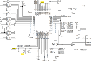
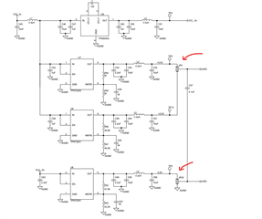
  • To configure the ADS1298ECGFE-PDK in bipolar mode, what configurations need to be made? I have already changed the positions of JP2 and JP20, but I am unable to understand the statement mentioned in the User's Guide sbau171d Section 5.2 Power Supply

    "The EVM is shipped in +3V unipolar supply configuration. The ADS1298 can operate in a single supply with +3.0V to +5.0V analog supply (AVDD/AVSS) or bipolar mode supply (±1.5V to ±2.5V).An additional digital supply of and +1.8V to +3.0V digital supply (DVDD) is required for operation."

  • The device ADS1298 can operate in a single supply with +3.0V to +5.0V analog supply (AVDD/AVSS) or bipolar mode supply (±1.5V to ±2.5V).

    For 3V unipolar configuration (through on-board LDOs), place jumpers on JP20 1-2; JP2 2-3

    For +/- 2.5 bipolar configuration (through on-board LDOs), place jumpers on JP20 2-3; JP2 1-2

    For other voltages supported by the device, you can remove the shunts on JP20 and JP2 and directly connect the voltages to JP20 pin 2 and JP2 pin 2.

  • Hi Praveen,

    Thank you for the clarification.

    I was able to test the board in bipolar mode, the results are pretty similar to the unipolar mode. The waveform still has a lot of distortion.

    While the test signals appear to be fine, external known sine waves, DC, or similar signals introduces distortion. What could be the cause of this issue?

  • Hi Lolo,

    Can you increase the data rate? Based on the register settings, you have the data rate of 500sps. For a 50Hz signal, you only get 10 samples per cycle. This is the reason for the signal to look distorted. 

    If you increase it to 8ksps data rate, you should not see the distortion.

  • Hi Praveen,

    I increased the data rate as you suggested, and the signals of 50Hz now appear to be pretty decent. Thank you for your inputs.

    Later, I started experimenting with different amplitudes and frequencies of signals ranging from 1mV to 10mV and 20Hz to 100Hz. I discovered that I have to change the data rate for different combinations. I was considering the Nyquist criterion, if I set the data rate to more than twice the highest frequency, the signal can be reconstructed. However, the situation here seems to be different.

    Could you please point out what I am missing here?

  • Hi,

    Sampling at twice the highest frequency isn't sufficient to fully reconstruct the sine wave signals. You will see distortion in the output signals as you noticed.

  • Thank you for your inputs. I have obtained proper sine wave signals with the help of a low pass filter for 8000Hz sampling.


    However, I am still facing issues with reconstructing accurate DC signals of low amplitude.
    I have configured the ADS1298ECGFE-PDK in bipolar mode and ensured that the signal falls within the common mode input range. Trying different datarates, the issue persists unlike with the sine wave signal. The DC signal of higher amplitude appears fine, but the low amplitude signal does not.
    What could be the problem? Please refer to the attached plot.

    dc_signal_issue.zip

  • Hi, what you are measuring is probably the channel DC offset which seems to be avg of about 1.8mV in your measurement across all the DC levels which can be calibrated out.