Other Parts Discussed in Thread: ADS1298,
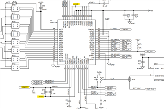
I am currently working with the ADS1298ECGFE-PDK and have connected a waveform generator to the input pins IN2. The positive end of the waveform generator is connected to IN2P, and the ground from the waveform generator is connected to IN2N. I have configured the following registers on the ADS1298.
| Register   | Address | Value |
|------------|---------|-------|
| ID         | 0x00    | 0x92  |
| CONFIG1    | 0x01    | 0x86  |
| CONFIG2    | 0x02    | 0x10  |
| CONFIG3    | 0x03    | 0xDC  |
| LOFF       | 0x04    | 0x03  |
| CH1SET     | 0x05    | 0x91  |
| CH2SET     | 0x06    | 0x10  |
| CH3SET     | 0x07    | 0x91  |
| CH4SET     | 0x08    | 0x91  |
| CH5SET     | 0x09    | 0x91  |
| CH6SET     | 0x0A    | 0x91  |
| CH7SET     | 0x0B    | 0x91  |
| CH8SET     | 0x0C    | 0x91  |
| RLD_SENSP  | 0x0D    | 0xFF  |
| RLD_SENSN  | 0x0E    | 0x02  |
| LOFF_SENSP | 0x0F    | 0xFF  |
| LOFF_SENSN | 0x10    | 0x06  |
| LOFF_FLIP  | 0x11    | 0x00  |
| LOFF_STATP | 0x12    | 0x00  |
| LOFF_STATN | 0x13    | 0x02  |
| GPIO       | 0x14    | 0x00  |
| PACE       | 0x15    | 0x00  |
| RESP       | 0x16    | 0xF0  |
| CONFIG4    | 0x17    | 0x22  |
| WCT1       | 0x18    | 0x0A  |
| WCT2       | 0x19    | 0xE3  |
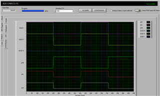
I applied sine and DC wave signals with amplitudes of 1mV, 5mV, and 10mV, along with frequencies of 10Hz, 25Hz, and 50Hz. However, I have encountered the following issues:
1. The waveform are getting distorted.
2. Clipping is observed, and the DC signal isn't a flat line; instead, there is a significant amount of deviation.
3. The signals are shifted from the zero line.
Can you guide how to resolve these issues. Could you please advise if the testing method is correct, or if there is something crucial that I might be missing?
Attached is the file containing graphs and signals.