This thread has been locked.

If you have a related question, please click the "Ask a related question" button in the top right corner. The newly created question will be automatically linked to this question.

ADC12DJ5200RFEVM: EVM tab - FPGA Reference Clock division factor

Part Number: ADC12DJ5200RFEVM
Other Parts Discussed in Thread: LMK04828

In ADC GUI,

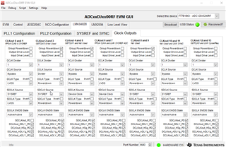
At "EVM" tab, I do see "FPGA Reference Clock" has a division factor of 20 (default) from input provided in "#2b. External FS Selection"

For example:

#2b. External FS Selection  = 4000

FPGA Reference Clock = 200

Question, Is it possible to modify this division factor in ADC GUI itself to a new number (like16 instead of 20)?

Best

Behrang

  • Hello Behrang,

    The FPGA Reference clock is not a divide down version of the external Fs, it is a divided down version of the SERDES rate, which is dependent on Fs. You can use the following equations to calculate the SERDES rate and the FPGA reference clock. And the fgpa ref clock divider also depends on what JMODE you are in wheter it is an 8b10b or 64b66b mode. If it is 8b10b the divider will be 40, if it is 64b66b it will be 66.

    JMODE0, 8b10b mode

    Fs=4000MHz

    SERDES rate = Fs * r = 4000 * 4 = 16000 MHz

    FPGA ref clock = SERDES rate / 40 = 400 MHz

    The FPGA ref clock dividers are by default set to 1, so whatever frequency you provide at sma input REF CLK is just distributed to all the LMK04828 clock outputs which then go to the FPGA. If you want to modify the dividers in the EVM gui go to the LMK04828 tab then the Clock outputs tab and you should see the screen I have shown below. Then you can vary the DCLK Divider dropdown to whatever divider setting you want. I would double check the ADC EVM schematic to ensure you are changing the correct LMK clock outputs. 

    best,

    Eric Kleckner