Hello,
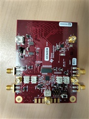
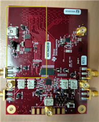
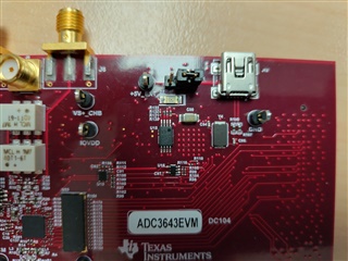
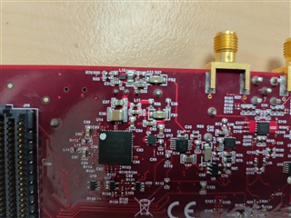
I'm currently trying to configure the ADC3643EVM with a Xilinx ZC702 FPGA.
To do so, I need to use the SDIO_I, SDIO_O, SEN, SDIO_OE and SCLK pins of the FMC connector.
In the schematic provided, these pins are connected to the ADC through resistors R90 to R94 and R96 to R100 must be unsoldered, is this correct?
However, I don't see resistors R90 to R94 on my board, are there any modifications between the gerber and the schematics provided and the current version of my board (REV E)?
And if so, are there any other important modifications to highlight ?