This thread has been locked.

If you have a related question, please click the "Ask a related question" button in the top right corner. The newly created question will be automatically linked to this question.

ADS131A02: After initialization, data is not changed.

Part Number: ADS131A02
Other Parts Discussed in Thread: ADS131A04

Hello,

I use ADS131A02 with microcontroller and I have problem with data channel. I read always 0x7FFFFF for the data channel.
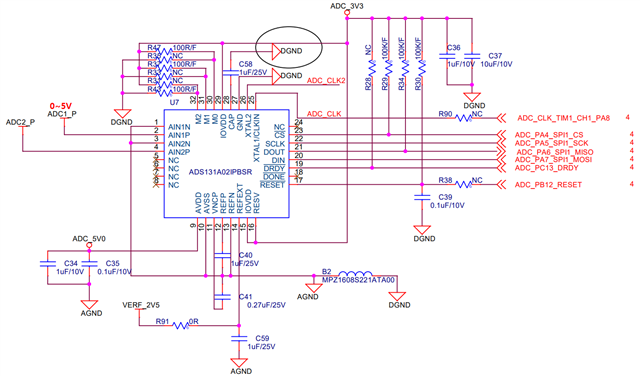
My Configuration:

M0 = IOVDD (Asynchronous interrupt mode)

M1 = IOVDD (32bits word length)

M2 = GND (Hamming data off)

Interface mode : Asynchronous interrupt mode

fCLKIN : 16.384MHz X-tal

Reading and writing registers works correctly and when I send command, I receive correct ACK.

Initialisation set up:

  • Power Enable
  • Reset
  • Send NULL 16bit value(0x0000) and I receive 0xFF02.
  • UNLOCK command and I receive 0x0655.
  • Configuration each registers(A_SYS_CFG = 0x4B60(default), D_SYS_CFG = 0x4C3C(default), CLK1 = 0x4D02(fCLKIN/2), CLK2 = 0x4E20(fICLK/2, fMOD/4096, 1kHz fDATA), and I receive each response 0x2XXX.
  • Enable all channel(0x4F0F) and I receive 0x2F03 (Is this OK? or must received 0x2F0F?)
  • WAKEUP command and I receive 0x0033.
  • LOCK command and I receive 0x0555.

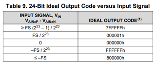
When DRDY pin falling interrupt, I receive 0x7FFFFF data always.

When I change input voltage, data is not changed. Always 0x7FFFFF or 0xFFFFFF.

What is the problem?

Thanks,

  • Hi SeungSang,

    For your question "Enable all channel(0x4F0F) and I receive 0x2F03 (Is this OK? or must received 0x2F0F?)",

    My answer:  0x2F03 is a correct response from ADS131A02 for your 0x4F0F command because ADS131A02 has only 2 input channels, You will get the same response if you send 0x4F03 command to your ADC.  0x2F0F response should be expected only for ADS131A04 ADC.

    Is there any specific reason you configured this ADC for 32-bit word length? If 32-bit word size is selected, you must send each word with 32-bit length. It would be good if you could share your timing plot for SCLK, DIN, DOUT,/DRDY and /CS. Also, you can change it to 24-bit word size but you also need to send 24-bit size for each command and NULL.

    BR,

    Dale

  • Thanks Dale,

    I send SPI word length 32bits. 0xXXXX0000.

    When I send to ADC, I attach zero(2bytes).

    And when I receive response, I catch the first 2 bytes data.

    My init sequence is below, plz check and help, catch the problem.

    The direction from left to right indicates the flow of time.

    DOUT is MISO pin, DIN is MOSI pin.

    And these are same time data.

    I think the yellow mark is suspicious. But I don't know why.

    BR,

    SeungSang

  • Hi SeungSang,

    It is not easy to understand what you shared without more information because the ADC always responds the previous command, so my first question is, are the data you are showing the data for a couple of frames? You are showing 11 words(32-bit) which are more than the data required for one frame. It would be good if you can include SCLK,/CS and /DRDY signals.

    BR

    Dale

  • Hi Dale,

    My problem is solved(?).

    I supply to Vref 5V, not 2.5V.

    All register setting is OK with SPI. And output data is changed with power supply input.

    But I have a new problem.

    If I input 5.0V, ADC output  0x7FFFFF. And input 0.0V, then ADC out 0x000000.

    These are 23bit resolution.

    I want to use 0~5.0V range, 24bit resolution.

    How can I use? What things do I need to change?

    BR,

    SeungSang

  • Hi SeungSang,

    I did not see your schematic, however you can use pseudo-differential input configuration (Vcm=2.5V) as below if your signal is 0~5V single-ended input and Vref is 2.5V.

    BR,

    Dale

  • Hi Dale,

    Thanks for your help.

    Plz review our schematic, below. Are you sure we are using pseudo-differential input mode?

    I have no knowledge of schematic. I am a software engineer.

    And I have a question.

    If we use pseudo-differential input mode, ADC output data range is 0x000000(0V) ~ 0xFFFFFF(5V) ?

    Please review our schematic and then reply.

    BR

    SeungSang

  • Hi Hi SeungSang,

    From your schematic, you are not using pseudo-differential input. A single +5V power supply is used, internal negative charge pump is disabled (A_SYS_CFG = 0x60 default value), external Vref=2.5V is selected, and also AINN is tied to ground, so ADS131A02 ADC measures the differential voltage VIN = VAINP – VAINN, the input range is -VREF/Gain to +VREF/Gain which is -2.5V to +2.5V as your Gain=1 by default. 

    When you applied a +5V to AINP, the differential voltage is VINP-VINN=5-0=5V, this has exceeded the maximum input range (+2.5V) according to your schematic and configuration, so what you saw (If I input 5.0V, ADC output  0x7FFFFF. And input 0.0V, then ADC out 0x000000) is correct. You will always see 0x7FFFFF when your input voltage to AINP is between +2.5V and +5V. If you want to measure a signal between 0V and +5V, you should connect a 2.5V DC to AINN pin which is pseudo-differential input as the block diagram shown in my previous post.

    Also, using a ferrite bead between AGND and DGND is not a good design, a solid ground plane is recommended, please see the layout guideline in the data sheet.

    BR,

    Dale