ADS127L11: Front end for ADS127L11

Part Number: ADS127L11
Other Parts Discussed in Thread: INA849, TPS65130, INA851, TPS7A39

Hello,

I am starting a new design for an acquisition system with up to 32 channels isolated to each other. Each channel block will have an isolated DCDC and an ADS127L11 ADC. I am now at the stage that I would like to define the front-end for the ADS127L11 and I am facing some design changes and would like to ask about your recommendation for possible setups. Below you can find the requirements:

- As each channel is isolated from each other I do not have any excessive CMMR requirements

- Input impedance of 1GOhm

- Measurement range of +/-10V

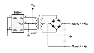
- If possible the output of the isolated DCDC should be 5V 

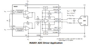
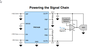
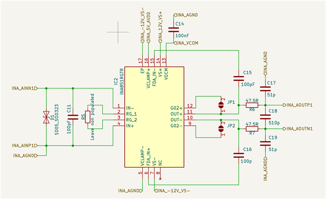
Looking at the requirements the most obvious choice could be an INA instrumentation amplifier. The issue is that I would need bipolar supplies. I am wondering, as I have seen in other commercial products with exactly the same requirements with the exception of the usage of a 16bit ADC and without instrumentation amplifiers, if there is a way either to avoid the bipolar supplies or to generate them out of the 5V main supply in a very simple way. I have a very small space in layout for each one of the channels and therefore area is of the essence. Furthermore the instrumentation amplifiers tend to be quite cost intensive.

Thanks in advance for your support and Best Regards,

Javier

  • Hello Javier,

    If you need 1GOhm, the only practical approach is an instrumentation amplifier, or some other input buffers, requiring +/-12V to +/-15V supplies.  You can use a passive input resistive divider to support a 5V only power supply, but in order to get low noise and decent bandwidth/settling time, the maximum impedance is 1MOhm, and for 20b or higher applications, the maximum impedance is usually 100kOhm or lower.

    I would suggest looking at the INA849; this device can directly drive the ADS127L11 inputs.  However, as you pointed out, this device will require higher voltage bipolar supplies.

    Since you will have an isolated 5V supply, you can generate +/-15V supplies using the TPS65130.

    Another option is to use a transformer driver with dual outputs such as SN6501.

    Signal and Power Isolation with 3.3 V / 5 V Input and 12 V / 15 V Output

    Regards,
    Keith Nicholas
    Precision ADC Applications

  • Hello Keith,

    as always, thank you very much for your support. I will then go with the instrumentation amplifier. On that regards I have some questions:

    1- The INA849 has a minimum gain of 1. For my application this would be problematic as I have to attenuate the input signal from +/-10V to the range of the ADS127L11. Do you agree or do you see a simple way to attenuate with reasonable noise?, if none, shall I then go for the INA851 (which luckily I have in another design already :)) and set the gain to 0.2. For me the INA849 offers some advantages during prototyping (the SOIC/VSSOP package).

    2- As I have to use an isolated DCDC anyway I could go for one with +/-12V output and then use an LDO to generate the 5V for the AVDD supply of the ADS127L11 (as it has very low consumption the losses of the LDO shall not be a big deal) and out of the first LDO to generate the 1.8V for IOVDD. Do you think this configuration would be ok from the noise point of view?, any suggestions to filter the output of the DCDC for the INA?

    3- Do I have to bias the INA851 inputs to the ground of the ADS? Is there an alternative (as I have to keep the 1GOhm requirement)?

    Regards,

    Javier

  • Javier,

    I will get back to you on Monday.

    Regards,

    Keith

  • Hello Javier,

    1.  I showed a picture of the INA851, but I mis-stated using the INA849; not sure why I mixed those two devices up!  Yes, INA849 will only support a minimum gain=1.  If you use the INA849, you will need to use a voltage divider on the output and then buffer this before driving the ADC input, requiring an additional amplifier stage.  I would suggest using a fully differential amplifier to drive the ADC input and provide the necessary common mode voltage at this point.  Or, use the single INA851 which integrates the instrumentation input and a differential ADC driver output stage in a single device, support a minimum gain of 0.2.

    2.  Yes, you can generate all required supply voltages using a dual bipolar supply and voltage regulators.  For best performance, I would suggest using +/-15V supplies feeding low noise LDOs that then regulate the voltage to +/-12V.  You may not need this extra regulation, but it will give you the overall best noise performance.  TPS7A39 is a dual LDO designed for this use case.

    3.  Since each of your channels are isolated from each other, you do not need to use a differential input configuration.  You can simply tie the negative input of the instrumentation amplifier to the channel isolated ground.  The channel input will then be an isolated, single-ended input with respect to the isolated ground.  In this case, you do not need to add any biasing resistors.  However, you will want to add a passive input filter and some type of input protection for a robust design.  We have several reference designs that discuss this topic in more detail, including https://www.ti.com/tool/TIDA-01438.

    Regards,
    Keith

  • Hello Keith,

    thanks a lot for your answer. Sorry for the late reply, I was on holidays with little access to my emails/internet. I will then implement the INA851 and include your suggestion of the TPS7A39, as well as use a single-ended configuration. I will try to draft the schematic soon and share it with you here to assure that I have not made any mistakes.

    Regards,

    Javier

  • O.K.  Sounds good.

  • One fast question. Do you see any issue by using a 2.5V REF5025IDR (High-Grade) instead of an REF6225IDGKT with the ADS127L11? It would reduce my BoM costs to some extent.

    Regards,

    Javier

  • Hello Arijav,

    I have not looked at using this specific reference, but yes, you should be able to use it as long as you enable the REFP buffer inside the ADS127L11.

    Regards,
    Keith

  • Thanks Keith. Below you can find my proposal for the INA851 front end. As it is single ended and I need the highest possible impedance I have just added a TVS diode at the input and a 100pF capacitor. If you have any other proposal to improve filtering or protection against over voltage let me know.

    Best Regards,

    Javier

  • Hello Javier,

    I suggest adding an input resistor before D1 and C11.  This will limit current during an over-voltage condition, such as an ESD event.  100Ohm will not increase noise, and 1kOhm will have minimal impact on noise, especially for a gain=1 configuration.  

    Also, I do not see power supply bypass capacitors.  You should place 100nF near the supply pins, as shown in the suggested layout in Figure 9-14 of the INA851 datasheet.

    Regards,
    Keith

  • Hello Keith,

    thanks for your comments. I have added a 100Ohm resistor in the input. The bypass caps were located in another part of the schematic sheet, they are present Slight smile

    Regards,

    Javier