This thread has been locked.

If you have a related question, please click the "Ask a related question" button in the top right corner. The newly created question will be automatically linked to this question.

ADC12DJ5200RFEVM: JMode1 sync frame

Part Number: ADC12DJ5200RFEVM
Other Parts Discussed in Thread: TI-JESD204-IP,

Hi, 

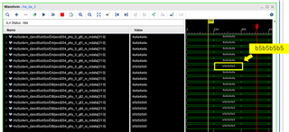
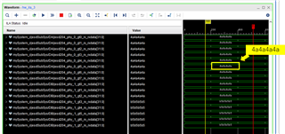
When communicating with JESD204B using JMODE1 (2 links, 16 lanes), the rx_start_of_frame values of two JESD204 PHY IPs are out of phase. Is this a reasonable guess?

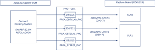
GBTCLK0 and GBTCLK1 are out of phase

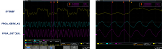
The frame timing of the two links (DA, DB) appears to be out of sync.

GBTCLK0 and GBTCLK1 are used for convenience on the FPGA side.
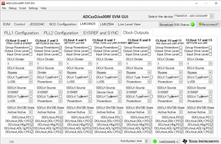
GBTCLK1 was default output OFF.
Is it possible to turn on GBTCLK1 by default?

Regards,
Takeo

  • Hello Takeo,

    If you are using the GUI it is not possible to change the default state it is programmed too, what I would recommend if you want to turn on GBTCLK1 you could perform this change in the GUI, save this configuration and then load instead of default programming. You could also alternatively also ensure that all clocks are set correctly before trying to bring up the link.

    Best,

    Eric

  • Hi Eric,

    Thanks for getting back to me so quickly.

    >>you could perform this change in the GUI, save this configuration and then load instead of default programming.
    Sorry, I do not see anything that looks like it in the menu bar of the GUI.

    Perhaps this is it?

    I will give it a go.


    Regards,

    Takeo

  • Hello Takeo,

    Yes correct to save a configuration you can go to the low level tab and then click the floppy disk icon, then to load a configuration you can select the folder icon which will open a file dialog and you can select the config file.

    Best,

    Eric

  • Hi Eric,

    OK, thank you very much.
    I was able to save and load the parameters !!

    By the way, has the new TI-JESD204C-IP been released?
    I was told by Ameet that it is scheduled for January 2024.


    Sorry, we are off the topic.
    But I would like to know the situation.

    Regards,
    Takeo

  • Hello Takeo,

    We are working on the release of the new TI-JESD204C IP, the release date has been pushed back from January and is no scheduled for the end of April. Are you currently using an older version of the TI IP or is it a different custom IP?

    Best,

    Eric

  • Hello Eric,

    I understand that the release is scheduled for the end of April.

    Q. Are you currently using an older version of the TI IP or is it a different custom IP?
    A. We are using Xilinx JESD204 PHY IP and JESD204 IP or JESD204C IP. (It is an evaluation version) I was waiting in anticipation because TI's TI-JESD204-IP did not support Vivado 2023.x and I heard that the next release will support block designs.

    We are combining TI's ADC evaluation board with Hitech Global's FPGA evaluation board, which is probably not proven.
    That is where we are challenging ourselves, but it is not working.

    Setting
    ・TI - ADC12DJ5200RFEVM (Customized to onboard clocking option)
    ・HitechGlobal - HTG830 (Kintex Ultrascale XCKU115)  URL:www.hitechglobal.com/.../Virtex-UltraScale-FPGA.htm
    ・JMODE1(12bit, singlechannel, 2link 16lane, lanerate=10.4Gbps fpgaclk=260Mhz)

    Regards,

    Takeo

  • Hello Takeo,

    The new release of the TI JESD IP will support vivado 2023.x and the release will come with some pre built modes you can drop in and use. This will come at the end of April timeline.

    Additionally, we have not used this particular HTG board in the past but we have had success with other versions of their capture cards so I don't think this will be an issue.

    Best,

    Eric

  • Hello Eric,

    Thank you for the reply.
    It is to be released shortly!!

    >Additionally, we have not used this particular HTG board in the past but we have had success with other versions of their capture cards so I don't think this will be an issue.
    I see.

    As I mentioned in the title, I am trying to fix the problem of out of sync incoming data.
    the transceiver's rx_data signal is not stable.

    The following waveforms were taken while the test mode was running.
    I know that the DB0-7 of the EVM is bit flipped.

    I think the FPGA setting on the data receiving side is suspect,
    but is it possible for the transmitted data to be bit-flipped?

    First,

    After FPGA reset,

    Regars,
    Takeo

  • Hello Takeo,

    Can you please clarify what you mean by out of sync data? Can you please share what test mode you are putting the ADC into. This signal routing table shown in the user guide is only for TI captures cards and will not apply to the specific capture card you are using. The lanes might be in a different order or there might be some lane inversions. You are correct that all B channel lanes are inverted but it is best to check that this matches on your capture card as well.

    Best,

    Eric

  • Hello Eric,

    Thank you for listening to my problems.

    Q. Can you please share what test mode you are putting the ADC into.
    A. D21.5 test mode (JMODE1, FPGAClock=260MHz, SamplingFreq=10.4G, LaneRate=10.4G)

    Q. Can you please clarify what you mean by out of sync data?
    A. It is saying that the transmitted data is not being received. In D21.5 test mode, the transmitter (ADC) is sending 0xB5, but the receiver (FPGA) is receiving 0x4A.I don't understand why it is bit flipped sometimes. If the bits are always inverted, then it could be a misconnection of positive and negative differential signals.However, if the bits flip or do not flip every time it is moved, it does not seem to be a connection problem. You may not have ever heard of such an event before.

    Q. You are correct that all B channel lanes are inverted but it is best to check that this matches on your capture card as well.
    A. At least the B-channel lanes of the ADC12DJ5200RFEVM all have the differential signals P and N inverted out to the FMC+ connector. That is noted in the EVM user guide and I have also checked the schematic.

    8B/10B Valid Characters
    docs.amd.com/.../10B-Valid-Characters

    If we look at a 10-bit bit sequence of 8b/10b, if the alignment is off by one bit, then B5 becomes 4A.
    In other words, is the alignment adjustment not working?

    8bit 10bit
    D21.5 => 101_10101 (0xB5) 101010_1010
    D10.2 => 010_01010 (0x4A) 010101_0101

    1bit shift ... 010101_0101 => 101010_1010 => 0xB5

    Regards,
    Takeo