This thread has been locked.

If you have a related question, please click the "Ask a related question" button in the top right corner. The newly created question will be automatically linked to this question.

ADC12DJ5200RFEVM: Bit Pattern for JMODE1

Part Number: ADC12DJ5200RFEVM
Other Parts Discussed in Thread: ADC12DJ5200RF, TI-JESD204-IP

Hi, 

Now, I am puzzled by the gap between the datasheet and the reference design.

How is the JMODE1 data format handled in the transport layer?

The following is an excerpt of comments from the transport layer source code included with the reference design (SLWC120).

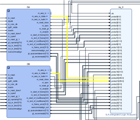
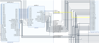
SourceFile:transport_ADC12DJxx00.v

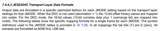
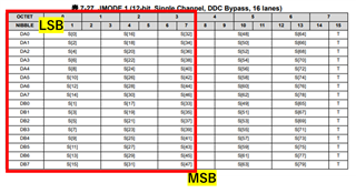
   // Bit pattern for JMODE1. Please refer ADC12DJxx00 datasheet for more details
   // Bit packing format is same for both JMODE1 and JMODE3. Please view this verilog file in notepad++ to have proper alignment of the table shown below
   // On 3rd link clock, 40 samples from first half of first frame is sent out- [S0, S1,.., S39] with S0 as MSB in rx_dataout signal
   // On the 4th link clock, 40 samples from second half of first frame is sent out- [S40, S41,.., S79] with S40 as MSB in rx_dataout signal
   // On the 5th link clock, 40 samples from the first half of second frame is sent out- [S0, S1, S2, …, S39] with S0 as MSB in rx_dataout signal and the sequence repeats
   // Out samples are delayed by 3 link clocks, due to internal registering
   
   
   /*  
	s0	31:20	s16	19:8	s32	7:0			31:28		s48	27:16	s64	15:4	3:0
	s2	63:52	s18	51:40	s34	39:32		63:60		s50	59:48	s66	47:36	35:32
	s4	95:84	s20	83:72	s36	71:64		95:92		s52	91:80	s68	79:68	67:64
	s6	127:116	s22	115:104	s38	103:96		127:124		s54	123:112	s70	111:100	99:96
	s8	159:148	s24	147:136	s40	135:128		159:156		s56	155:144	s72	143:132	131:128
	s10	191:180	s26	179:168	s42	167:160		191:188		s58	187:176	s74	175:164	163:160
	s12	223:212	s28	211:200	s44	199:192		223:220		s60	219:208	s76	207:196	195:192
	s14	255:244	s30	243:232	s46	231:224		255:252		s62	251:240	s78	239:228	227:224
	s1	287:276 s17	275:264 s33	263:256		287:284		s49	283:272	s65	271:260	259:256
	s3	319:308	s19	307:296	s35	295:288		319:316		s51	315:304	s67	303:290	291:288
	s5	351:340	s21	339:328	s37 327:320		351:348		s53	347:336	s69	335:324	323:320
	s7	383:372	s23	371:360	s39	359:352		383:380		s55	379:368	s71	367:356	355:352
	s9	415:404	s25	403:392	s41	391:384		415:412		s57	411:400	s73	399:388	387:384
	s11	447:436	s27	435:424	s43	423:416		447:444		s59 443:432	s75	431:420	419:416
	s13	479:468	s29	467:456 s45	455:448		479:476		s61	475:464	s77	463:452	451:448
	s15	511:500	s31	499:488	s47	487:480		511:508		s63	507:496	s79	495:482	483:480
	*/

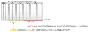
According to comments, LSB=> S32、MSB=>S15

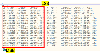
but, the ADC12DJ5200RF data sheet says that data is sent MSB first.

So I would think that MSB and LSB would be as follows.

LSB=> S0、MSB=>S47

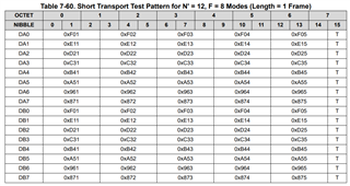
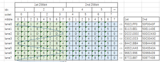
For example, I think the test pattern for the short transport layer will look like this.

What is the right thing to do?

I'm sorry I didn't make it clear enough. 

Regards,

Takeo

  • Hello Takeo,

    Can you please share a screenshot of what you are seeing in the ila on the fpga. The transport layer test pattern is shown in figure 7-60 for this mode but JMODE1 is a Dual edge sampling mode which means that the links will have to be interleaved in order to achieve the correct data. Once this is done the test pattern should read as shown below in the screenshot. As you can see sample one matches the transport layer mode and then the second sample is actually coming from sample 0 of channel B because they are being interleaved.

    best,

    Eric

  • Hello Eric,


    Sorry, this is the only information I can share with you right now.
    I am also having problems with RX Frame Error happening occasionally,
    so I think it contains a bit error.
    I would like to solve this problem too, but I don't know what to investigate.

    The DA_m_axis_rx_tdata and DB_m_axis_rx_tdata are output data from Xilinx JESD204 IP (Rx core).

    This is before breaking it down into the elements in the short transport test pattern table.

    DA
    508774385096643950a5543a50b4443b50c3343c50d2243d50e1143e50f0043f
    8772188796621996a5521aa5b4421bb4c3321cc3d2221dd2e1121ee1f0021ff0
    87721886906218b9a5525aafb4221bb4c3721c8350122c30605016e1f0000437
    87721886906218b9a5525aafb4221bb4c3721c8350122c30605016e1f0000437
    508774385096643950a5543a50b4443b50c3343c50d2243d50e1143e50f0043f
    8772188796621996a5521aa5b4421bb4c3321cc3d2221dd2e1121ee1f0021ff0
    4087743850966439d001503a50b4543b50c3343c50d2243d50e0143e50f0043f
    508774385096643950a5543a50b4443b50c3343c50d2243d50e1143e50f2057f
    :
    :
    :

    DB
    508774285096643950a5543a50b4443b50c3343650d2243d50e1143e50f0047d
    8772188796621996a5521aa5b4421bb4c3321cc3d2221dd2e1121ee1f0021ff0
    508774385096643950a5543a50b4443b50c3343c50d2243d50e1143e50f0043f
    50437c8f5096643171a7143b70b4443350531487d2521c515181143af0d007f8
    8772188796621996a5521aa5b4421bb4c3321cc3d2221dd2e1121ee1f0021fb2
    508774385096643950a5543a50b4443b50c3343c50d2243d50e1143e50f0043f
    8772188794625996a5521ab5b44252b3c3321cc3d2221dd271121ee1f0021ff0
    8772188796621996a5521aa5b4421bb4c3321cc3d2221dd2e1121ee1f0021fb2
    :
    :
    :

    Is this bit pattern correct? Is it wrong?

    The wiring is here.

    Regards,

    Takeo

  • Hello Takeo,

    The Xilinx JESD IP does the following:

    1> It concatenates the data of all the lanes to generate one output bus. For an 8 lane link, you will see a 256 bit bus (32 bits per lane per clock cycle)

    2> On each bus, the order of the bytes is reversed (to ensure that the first received byte is mapped to byte 0, the second to byte 1 and so on).

    To map the JESD IP output to the data you see in the JMODE table, kindly do the following:

    1> Separate the 256 bit bus into 8 32 bit segments. The lowest segment (31:0) will be for Lane 0, the highest (255:224) will be for Lane 7

    2> For each lane, byte reverse the data. You should now see the data map exactly as displayed in the JMODE table. Please note that in cases like JMODE0, where F=8, you need to accumulate two cycles of data on each lane (to create the 64 bit frame) in order to check the mapping of the data to the JMODE table. The 64 bit frame is also needed in order to identify the correct 4 tail bits that need to be discarded in each frame.

    After doing this please compare the transport layer test pattern table to your output.

    Thanks,

    Eric

  • Hello Eric,

    The data matches, Eric!
    When using TI-JESD204-IP, transport_ADC12DJxx00.v should be used.

    After all, what does the data conversion logic in transport_ADC12DJxx00.v mean?
    Am I to understand that the TI reference design does not use the Xilinx JESD204 PHY IP?

    Thanks,
    Takeo

  • Hello Takeo,

    No the TI JESD IP does not use the JESD204c PHY IP, in our custom designs the conversion from raw bytes to samples is taken care of for the user and all you would get out of the IP would be the ADC samples.

    Best,

    Eric

  • Hello Eric,

    >... all you would get out of the IP would be the ADC samples.

    That is very user-friendly for me.
    Thank you very much.

    Regards,
    Takeo