Other Parts Discussed in Thread: DAC38RF82, , LMK04828, LMK04832
Hello,
I am evaluating DAC38RF82 with the evaluation board (DAC38RF82EVM) and the TSW14J57 pattern generator.
A 100 MHz / +6dBm signal is fed to the input of the LMK (J4 connector).
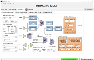
With the following configuration, all is right, it is possible to get a correct signal at the DAC output.
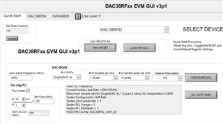
Now, the aim is to increase the DAC Clock Frequency in order to generate signal at the DAC output from 2000 MHz up to 3600 MHz.
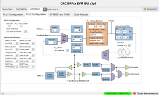
Always with a 100 MHz reference of the system, and using low PLL divider values (for good phase noise achievement), I want to work with a DAC frequency at 8800 MHz (frequency value in the frequency range of the highband VCO).
With the following configuration, the frequency of the signal to be fed to J4 connector on the evaluation board is 1100 MHz ! The purpose is to keep 100 MHz as the frequency reference...
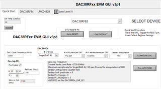
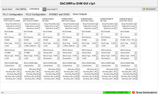
The number of lanes has been increased (from 4 to 8) in order to get a lower Serdes lane rate.
Can someone explain to me why a 1100 MHz signal is required in this case.
Is it really due to the DAC chip itself ?
Or is it due to the evaluation board architecture ?
Thanks for your help !
Alain