


Hi,
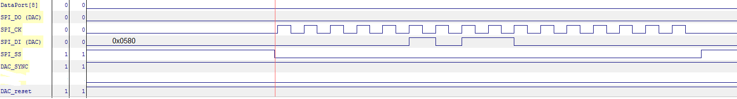
We are using DAC5688 in our design. We are communicating with DAC5688 on SPI but we are not successful. DAC5688 SPI is connected to TMS320DM6446 through FPGA. FPGA is acting as level translator. Physical connection from DSP to FPGA and FPGA to DAC5688 is correct, its monitored and analyzed by oscilloscope and chipscope.
The first step we are doing, enable the DAC5688 SPI as 4 wire interface.
dac5688_write (CONFIG5, 0x80); // To enable the DAC5688 SPI as 4 wire interface
Then we are trying to read the status of configuration register through SPI but we do not get valid data, always getting zero.
Here is the code
/*******************************************************************************/
#include "dac5688.h"
#include "spi_dm6446.h"
void main( void )
{
short i=0;
short low_i;
short hi_i;
char buff[31];
spi_init(); // initialize spi in 16bit mode
dac5688_write (CONFIG5, 0x80); // To enable the DAC5688 SPI as 4 wire interface
initDAC5688 (); // initialize dac5688
dac5688_read_all (buff); // reads all 31 registers
// implements sawtooth output from dac5688
while (1)
{
low_i = i & 0x00ff;
hi_i = i * 0x0100;
dac5688_write (CONFIG20, low_i);
dac5688_write (CONFIG21, hi_i);
}
}
/*************************************SPI******************************************/
void spi_init(void)
{
SYS_PINMUX1 |= 0x00000100;
/* Reset SPI */
SPI_SPIGCR0 = 0;
wait( 1000 );
/* Release SPI */
SPI_SPIGCR0 = 1;
/* SPI 4-Pin Mode setup */
SPI_SPIGCR1 = 0
| ( 0 << 24 )
| ( 0 << 16 )
| ( 1 << 1 )
| ( 1 << 0 );
SPI_SPIPC0 = 0
| ( 1 << 11 ) // DI
| ( 1 << 10 ) // DO
| ( 1 << 9 ) // CLK
| ( 1 << 1 ) // EN1
| ( 1 << 0 ); // EN0
SPI_SPIFMT0 = 0
| ( 0 << 20 ) // SHIFTDIR
| ( 0 << 17 ) // Polarity : when POL=1 dsp places data at rising edge
| ( 0 << 16 ) // Phase
| ( 81 << 8 ) // Prescale (81 for 1.0Mhz)
| ( 16 << 0 ); // spi word length in bits
spidat1 = 0
| ( 0 << 28 ) // CSHOLD
| ( 0 << 24 ) // Format [0]
| ( 2 << 16 ) // CSNR [only CS0 enbled]
| ( 0 << 0 ); //
SPI_SPIDAT1 = spidat1;
SPI_SPIDELAY = 0
| ( 8 << 24 ) // C2TDELAY
| ( 8 << 16 ); // T2CDELAY
SPI_SPIDEF = 0
| ( 1 << 1 ) // EN1 inactive high
| ( 1 << 0 ); // EN0 inactive high
SPI_SPIINT = 0
| ( 0 << 16 ) //
| ( 0 << 8 ) //
| ( 0 << 6 ) //
| ( 1 << 4 ); //
SPI_SPILVL = 0
| ( 0 << 8 ) // EN0
| ( 0 << 6 ) // EN0
| ( 0 << 4 ); // EN0
/* Enable SPI */
SPI_SPIGCR1 |= ( 1 << 24 );
}
unsigned short spi_cycle( unsigned short v)
{
Uint16 result;
// Clear any old data
SPI_SPIBUF;
//SPI access cycle
// Wait for transmit ready
while ( SPI_SPIBUF & 0x10000000 );
//wait (0x1000);
SPI_SPIDAT1 = ( spidat1 & 0x0ffcffff ) | v;
// Wait for receive data ready
while ( SPI_SPIBUF & 0x80000000 );
// Read 1 byte
result = SPI_SPIBUF;
return result;
}
/*******************************DAC********************************************/
short dac5688_read (char reg_addr)
{
// top bit in instruction word is for rd/wr
// for read operation the bit7 = 1
short instr = reg_addr | 0x8000;
return spi_cycle(instr);
}
void dac5688_read_all (char * buff)
{
unsigned short i;
for (i=0; i<31; i++)
{
//buff[i] = 0x00ff & dac5688_read (i);
buff[i] = dac5688_read (i);
}
}
short dac5688_write (char reg_addr, char value)
{
short instr = (reg_addr * 0x100) + value;
return spi_cycle(instr);
}
short dac5688_read_status (void)
{
// top bit in instruction word is for rd/wr
// for read operation the bit7 = 1
short instr = 0x8000 | STATUS0;
return spi_cycle(instr);
}
void initDAC5688(void)
{
char value;
// CONFIG1 Register
value = 0x00
| (1<<6) //insel_mode[1:0]; Farrukh.. Select A input for both channels
| (0<<5) //unused
| (0<<4) //synchr_clkin
| (1<<3) //twos; Farrukh.. 1=>twos complement
| (0<<2) //inv_inclk; Farrukh.. 0=>no inversion
| (3<<0); //interp_value[1:0]; Farrukh.. 3=>X8 interpolation
dac5688_write (CONFIG1, value);
// CONFIG2 Register
value = 0x00
| (0<<7) //diffclk_ena; Farrukh.. 0=>single ended clock
| (1<<6) //clk1_in_ena
| (0<<5) //clk1c_ in_ena; Farrukh.. 0=>Pin acts as PLL_LOCK status
| (0<<4) //clko_SE_hold
| (0<<3) //fir4_ ena
| (0<<2) //qmc_ offset_ena
| (0<<1) //qmc_ corr_ena
| (1<<0); //mixer_ena
dac5688_write (CONFIG2, value);
// CONFIG3 Register
value = 0x00
| (0<<6) //diffclk_dly(1:0)
| (0<<4) //clko_dly(1:0)
| (0<<0); //Reserved(3:0)
dac5688_write (CONFIG3, value);
// CONFIG4 Register
value = 0x00
| (0<<7) //ser_dac_ data_ena; Farrukh.. this can be set to test DAC from SPI
| (0<<5) //output_delay(1:0)
| (0<<4) //B_equals_A
| (0<<3) //A_equals_B
| (0<<2) //unused
| (0<<1) //reva
| (0<<0); //revb
dac5688_write (CONFIG4, value);
// CONFIG5 Register; Farrukh.. Leave at DEFAULT
value = 0x00
| (1<<7) //sif4
| (0<<6) //sif_ sync_sig
| (1<<5) //clkdiv_sync_ena
| (0<<4) //clkdiv_sync_sel
| (0<<3) //Reserved
| (0<<2) //clkdiv_shift
| (1<<1) //mixer_gain
| (0<<0); //unused
dac5688_write (CONFIG5, value);
// CONFIG6 Register; Farrukh.. Leave at DEFAULT
value = 0x00; // phaseoffset(7:0)
dac5688_write (CONFIG6, value);
// CONFIG7 Register; Farrukh.. Leave at DEFAULT
value = 0x00; // phaseoffset(15:8)
dac5688_write (CONFIG7, value);
// CONFIG8 Register
value = 0x0e; // phaseadd(7:0)
dac5688_write (CONFIG8, value);
// CONFIG9 Register
value = 0x2d; // phaseadd(15:8)
dac5688_write (CONFIG9, value);
// CONFIG10 Register
value = 0xb2; // phaseadd(23:16)
dac5688_write (CONFIG10, value);
// CONFIG11 Register
value = 0x0d; // phaseadd(31:24)
dac5688_write (CONFIG11, value);
// CONFIG12 Register
value = 0x00; // qmc_gaina(7:0)
dac5688_write (CONFIG12, value);
// CONFIG13 Register
value = 0x00; // qmc_gainb(7:0)
dac5688_write (CONFIG13, value);
// CONFIG14 Register
value = 0x00; // qmc_phase(7:0)
dac5688_write (CONFIG14, value);
// CONFIG15 Register
value = 0x00
| (0<<6) //qmc_phase(9:8)
| (4<<3) //qmc_gaina(10:8)
| (4<<0); //qmc_gainb(10:8)
dac5688_write (CONFIG15, value);
// CONFIG16 Register
value = 0x00; // qmc_offseta(7:0)
dac5688_write (CONFIG16, value);
// CONFIG17 Register
value = 0x00; // qmc_offsetb(7:0)
dac5688_write (CONFIG17, value);
// CONFIG18 Register
value = 0x00
| (0<<3) //qmc_offseta(12:8)
| (0<<2) //unused
| (0<<1) //unused
| (0<<0); //unused
dac5688_write (CONFIG18, value);
// CONFIG19 Register
value = 0x00
| (0<<3) //qmc_offsetb(12:8)
| (0<<2) //unused
| (0<<1) //unused
| (0<<0); //unused
dac5688_write (CONFIG19, value);
// CONFIG20 Register
value = 0x00; // ser_dac_data(7:0)
dac5688_write (CONFIG20, value);
// CONFIG21 Register
value = 0x00; // ser_dac_data(15:8)
dac5688_write (CONFIG21, value);
// CONFIG22 Register
value = 0x00
| (0<<6) //nco_sel(1:0)
| (1<<4) //nco_reg_sel(1:0)
| (1<<2) //qmcorr_reg_sel(1:0)
| (1<<0); //qmoffset_reg_sel(1:0)
dac5688_write (CONFIG22, value);
// CONFIG23 Register
value = 0x00
| (0<<7) //unused
| (0<<6) //unused
| (2<<3) //fifo_sel(2:0)
| (1<<2) //aflag_ sel
| (0<<1) //unused
| (1<<0); //unused
dac5688_write (CONFIG23, value);
// CONFIG24 Register
value = 0x00
| (0<<4) //fifo_sync_strt(3:0)
| (0<<3) //unused
| (0<<2) //unused
| (0<<1) //unused
| (0<<0); //unused
dac5688_write (CONFIG24, value);
// CONFIG25 Register is all unused
// CONFIG26 Register
value = 0x00
| (0<<7) //io_1p8_3p3
| (0<<6) //unused
| (0<<5) //sleepb
| (0<<4) //sleepa
| (1<<3) //isbiaslpfb_a
| (1<<2) //isbiaslpf_b
| (0<<1) //PLL_ sleep
| (1<<0); //PLL_ena
dac5688_write (CONFIG26, value);
// CONFIG27 Register
value = 0x00
| (15<<3) //coarse_daca(3:0)
| (15<<0); //coarse_dacb(3:0)
dac5688_write (CONFIG27, value);
// CONFIG28 Register is Reserved
// CONFIG29 Register
value = 0x00
| (8<<3) //PLL_m(4:0)
| (1<<0); //PLL_n(2:0)
dac5688_write (CONFIG29, value);
// CONFIG30 Register
value = 0x00
| (0<<7) //PLL_LPF_ reset
| (0<<6) //VCO_div2
| (1<<4) //PLL_gain(1:0)
| (1<<0); //PLL_range(3:0)
dac5688_write (CONFIG30, value);
}
Waiting for quick reply, because its delaying our projects.
Regards

 .
.
