ADS5296A: Test Pattern Generation;Frame Clock;Bit Clock

Part Number: ADS5296A

Tool/software:

Hello,

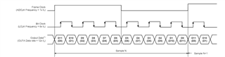
I am integrating the ADS5296A into my design with a 160 MHz input clock and am trying to generate a 12-bit Ramp Test Pattern. Unfortunately, I am not seeing any output from the ADC, and the interleaved mode is enabled in my setup.

I have a few concerns and would greatly appreciate your guidance on the following:

1. What should the frame clock rate be? Should it match the input clock or be half of it? When I probe the clock, it is unstable, varying from 65 MHz to 80 MHz.

2. Could you please confirm the specific registers I need to configure to initiate the Ramp test pattern? Is there a specific sequence of writes I need to follow? Below are the register writes I have attempted:

- 00h: 0001h
- 00h: 0000h
- 07h: 0001h
- 40h: 8000h
- 45h: 0000h
- 46h: 8208h
- 25h: 0140h

Thank you for your assistance.

Best regards,
Akshit

  • Also, interested in knowing the rate of bit clock and it's relation with input clock.

  • Hi,

    In the interleaving mode if the input clock is 160 MHz .Each ADC converts sample on alternating sample . 

    1) Frame clock will be half of the ADC_Clock . 80 MHz is the expected frame clock in your case

    Bit clock to frame clock relation is shown in the below diagram.

    I dont see any problem with register setting . Few questions 

    1) Are you trying this on EVM or your custom board ?

    2) Did you verify the register write is happening properly ? You can readout the registers to verify .

    3) Can you check all supplies have sufficient current range . You can probe on all supply to check whether they are getting expected voltage

    4) You are seeing no ouput from dout is that correct ? Is it problem only in interleaving mode or you  tried only this mode ? This is just to understand your problem.

  • Hi Sachin,

    Thank you for the reply and clarification. 

    Please find my answer below:

    1) Are you trying this on EVM or your custom board ? --This is our custom board.

    2) Did you verify the register write is happening properly ? You can readout the registers to verify . -- Yes I have verified them and the chip returns the same value I wrote. 

    3) Can you check all supplies have sufficient current range . You can probe on all supply to check whether they are getting expected voltage --Voltage were okay when probed but will verify against datasheet for current

    4) You are seeing no ouput from dout is that correct ? Is it problem only in interleaving mode or you  tried only this mode ? This is just to understand your problem. --What do you mean by dout? Dout of serial interface or output for the converter? We do see something out from the output but it looks noisy and do not make it weather it is correct or not. I tried changing the setting on register 25h to use different patterns. Output seems to change based on that but it is very noisy to determine if it is behaving correctly or not?

     
    My question is what is expected from Test_Patt0: 1 = Enables a mode where the output is a constant specified code; ensure that bits D5 and
    D6 are '0'? Is it going to output a constant value? If yes what is the expected value we should see on the output? 

    Thank you,
    Akshit

  • I also read all the register from ADC after setting up:

    Address Data
    00h 0
    07h 1
    0Ah 0
    0Fh 0
    14h 0
    1Ch 0
    23h 0
    24h 0
    25h 40
    26h 0
    27h 0
    29h 0
    2Ah 0
    2Bh 0
    2Ch 0
    2Dh 0
    2Eh 0
    2Fh 0
    30h 0
    31h 0
    32h 0
    33h 0
    34h 0
    35h 0
    38h 0
    40h 8000
    42h 44
    45h 0
    46h 8208
    50h 210
    51h 543
    52h 76
    53h 567
    54h 234
    55h 1
    5Ah 3
    5Bh 0
    5Ch 5
    5Dh 1
    5Eh FE5
    5Fh FFE
    60h 49
    61h 3
    62h F4E
    63h FFC
    64h 27C
    65h 400
    66h 3
    67h 0
    68h 5
    69h 1
    6Ah FE5
    6Bh FFE
    6Ch 49
    6Dh 3
    6Eh F4E
    6Fh FFC
    70h 27C
    71h 400
    72h 3
    73h 0
    74h 5
    75h 1
    76h FE5
    77h FFE
    78h 49
    79h 3
    7Ah F4E
    7Bh FFC
    7Ch 27C
    7Dh 400
    7Eh 3
    7Fh 0
    80h 5
    81h 1
    82h FE5
    83h FFE
    84h 49
    85h 3
    86h F4E
    87h FFC
    88h 27C
    89h 400
    8Ah 3
    8Bh 0
    8Ch 5
    8Dh 1
    8Eh FE5
    8Fh FFE
    90h 49
    91h 3
    92h F4E
    93h FFC
    94h 27C
    95h 400
    96h 3
    97h 0
    98h 5
    99h 1
    9Ah FE5
    9Bh FFE
    9Ch 49
    9Dh 3
    9Eh F4E
    9Fh FFC
    A0h 27C
    A1h 400
    A2h 3
    A3h 0
    A4h 5
    A5h 1
    A6h FE5
    A7h FFE
    A8h 49
    A9h 3
    AAh F4E
    ABh FFC
    ACh 27C
    ADh 400
    AEh 3
    AFh 0
    B0h 5
    B1h 1
    B2h FE5
    B3h FFE
    B4h 49
    B5h 3
    B6h F4E
    B7h FFC
    B8h 27C
    B9h 400
    BEh 83
    F0h FFFF

    What I am not getting here is why F0h is FFFF. I tried writing to '0' explicitly with other registers. Also, some of the values are non-zero which I am not even changing that. Example is register 42h which 44h instead of 0.


  • What I meant by dout is outx_p/outx_n . How are you looking at the output ?  In each output pin the 12 bits of a sample comes serially . So you need to construct a 12 bit value by combining those . In the ramp mode these 12 bit values will increment linearly .


    Test_Patt0: 1 = Enables a mode where the output is a constant specified code; ensure that bits D5 and
    D6 are '0'?

    This means in register 25 bit5 and bit6 should be written as zero . This will give constant code test pattern.

    On powerup some register values are set to 1 so you might see non zero values in some register.

    Register F0 MSB is mentioned in datasheet as External Reference mode . This has to be zero if you are not giving external reference . You had already tried writing 0 to F0h and getting FFFFh . MSB bit being 1 is not expected as you are not setting this to 1 . Can you please look at  your SPI protocol ? When you write this register you can probe the spi lines to see everything is as expected .

  • I have the FPGA on the other end to acquire the data and serially collects the data and constructs it to 12 bits. I am also probing the output to see if it is linearly incrementing. 

    What is meant by constant code? 

    Almost all registers by default is set to '0' after reset according to datasheet. So not sure why some of the registers are non-zero when read? It looks like my Serial interface is working correctly as I can read what I wrote.  I will re-check it though. 

  • Akshit ,

     If you make TESTPAT0 (Bit D4  in register 25h) then BIT_CUSTOM1 register programmed value will come at the output .

    There can be some readonly register . Eventhough if you write 0 it may not reflect back. But in your case I see even the registers which in mentioned in datasheet is showing 1 eventhough you are not programmin it to 1.

    For example 1) F0h MSB bit    2) 42h bit 6

    Please recheck your spi again .

  • Hi Sachin,
    Apologies for delayed response. I have verified that there is no issues with my SPI writes and Read. 

    But I did find out that the ISERDES primitive from AMD/Xilinx required clock in a particular manner. After changing the logic around it, I can get the ramp test pattern. 

    My other question is if I want to use  BIT_CUSTOM1 register, is this the right registers writes for it? 

    - 00h: 0001h
    - 00h: 0000h
    - 07h: 0001h
    - 26h: 0000h
    - 40h: 8000h
    - 45h: 0000h
    - 46h: 8208h
    - 25h: 0111h

    OR

    - 00h: 0001h
    - 00h: 0000h
    - 07h: 0001h
    - 26h: 0040h
    - 40h: 8000h
    - 45h: 0000h
    - 46h: 8208h
    - 25h: 0111h

    OR


    - 00h: 0001h
    - 00h: 0000h
    - 07h: 0001h
    - 26h: 0040h
    - 40h: 8000h
    - 45h: 0000h
    - 46h: 8208h
    - 25h: 0113h

    Do you know what is the expected value if 26h register value is x0000 and the value is x0040? 

    Thank you

  • Akshit ,

    Good to know your ramp pattern issue solved . But we were seeing the read register was not matching with whatever we wrote . Please check that again as in future there is no need to doubt spi again.

    Once you write in 25h Bit4 (TEST_PATT0) to 1 - it is in constant specific code mode. 

    This constant specific code is 12 bit code which can be set using register 25h (BITS_CUSTOM1[11:10]) and 26h (BITS_CUSTOM1[9:0])  by user.

    Below is the expected output for your 3 cases 

    1) 0100 0000 0000

    2) 0100 0000 0001

    3) 1100 0000 0001

  • Yes, those register still do not read correctly. So I do not think it is my SPI bus. Since what I wrote is I can read it back correctly. AS an example I wrote 8020h to register 42h and read I back 8020h as well as I saw the phase of LCLK changing which matches the datasheet. It is only some registers which are not giving the default values then it should be. 
     

  • Ok, Understood. 

  • HI Sachin,
    Continuing this thread, I would like to know what is the output format when ramp pattern test in initiated for Out1 and out2 if ADC is in interleaved mode?

    Out1 and out2 will give same output or one will have be ahead of another. Example: Out1 = x"001" and Out2 = x"001" or Out1 = x"001" and Out2 = x"002".

    Thank you!

  • I also would like to know about external Sync signal and how it is used?

    Does it need to be 1 clock wide? Can it be continuous? is it Twice the frequency of Input frequency?

    What is the sequence to enable TP_HARD_SYNC Bit 15 of register 25h? Does it need toggle once? or it has be high always?