ADS1299EEGFE-PDK: Powering and communication of ADS1299FE Daughter board with Arduino

Part Number: ADS1299EEGFE-PDK
Other Parts Discussed in Thread: ADS1299

Tool/software:

Hi, 

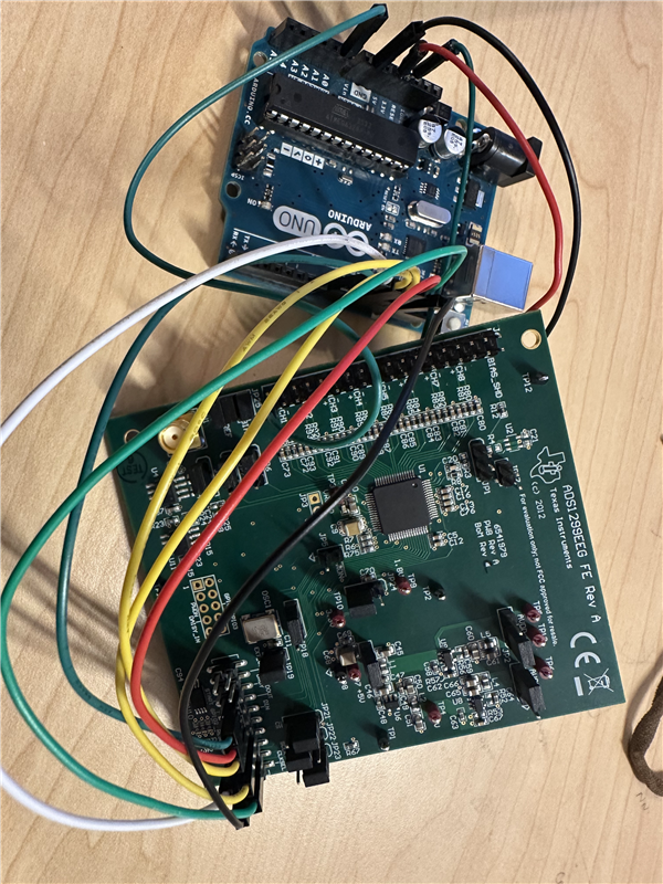
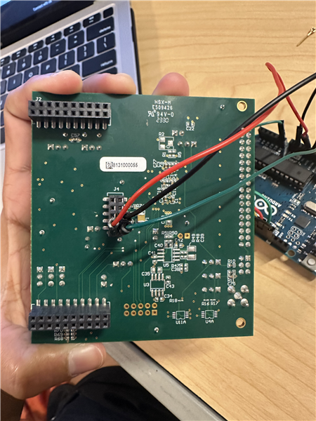
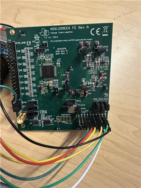
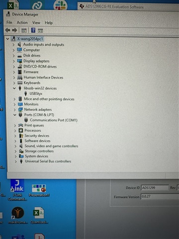
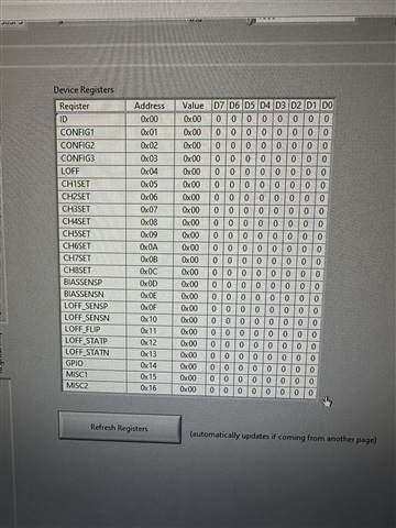
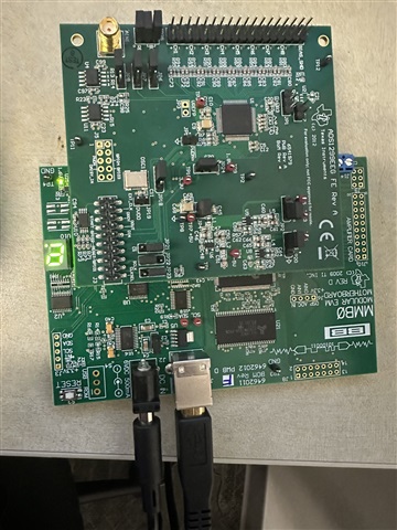
I am trying to interface the ADS1299EEG FE with an Arduino.

Do I need to keep the MMB0 on for power supply to the ADS board, or can I  simply use the Arduino for supplying power to the daughter board and for SPI communication? 
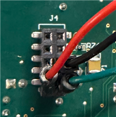
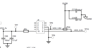
In case of the latter, can I simply connect a jumper cable from Arduino  5V to AVDD (JP2) on the ADS1299EEG FE daughter board?

 Is there any documentation available for making these connections?

.........                                         

  • Hello Meghna,

    Thank you for your post.

    The ADS1299EEG-FE daughter board can be used as a standalone platform with another microcontroller. Power supplies and digital communication signals can be connected to the available test points or header pins. Be sure to share both power supplies and GND connections. You may refer to the User Guide for documentation about the hardware design.

    Regards,

    Ryan

  • Hello Ryan,

    Thank you for your reply.

    However, using the J4 connector, I'm unable to get 1.8V in TP9. Other test point voltages are fine. All the other jumpers are in default mode as per the User Guide. Please let me know what I'm missing here.

    Here's the picture of the connections:

  • Hello Meghna,

    Can you confirm which pins the wires on J4 are connected to? It's difficult to distinguish the rows clearly.

    It looks like red wire is connected to J4.10 - I assume this is 5 V? Please recheck the green and black wire connections (I assume these are 1.8 V and GND). Since you are not using the MMB0 mother board, you can connect the green wire to either pin 7 or 9 and configure the JP24 jumper accordingly.


    Regards,

    Ryan

  • Hi Ryan,

    The red wire (J4.10) is 5V.
    The green wire(J4.9) is 3.3V and black is the GND.

    With the J24 being shorted in 2-3 and the other Jumpers as shown in the above pictures, I'm assuming that I should be able to read/write the register values? Or am I missing anything here?

  • Hi Meghna,

    You mentioned that you were unable to get 1.8V in TP9, so I assumed you were trying to use this as your DVDD supply. There is no need to measure 1.8 V on TP9 if you are using 3.3 V for DVDD with JP24 in the [2-3] position. The supply connections look correct now.

    Regards,

    Ryan

  • Hi Ryan, 
    I am not able to Read/Write any Registers using Arduino. It's all zero.

    I also tried with the MMB0 board but I'm unable to progress.  I've been following this link, but there still seems to be an error.

    This is the screenshot of my device manager:

    This is the screenshot of the register values:

    This is my hardware:

    Is there any updated instructions for the smooth operation of EVM GUI?

    At present, I am just installing ADS1299EEGFE-PDK-SW. Do I need to install all 3 or only the 3rd one?

  • Hi 

    Is there any update?

  • Hi Meghna,

    You do not need either of the two software source code downloads to operate the EVM.

    When using MMB0 + EVM together, please start by configuring all jumpers in their default setting according to section 2.5 of the User Guide. It looks like JP18 is missing a jumper, which would enable the on-board oscillator (external clock input to the ADS1299 CLK pin). 

    The 'e' on the MMB0 7-segment display indicates that the GUI failed to initialize the EVM. This is likely due to the missing jumper on JP18. I also suggest the following procedure to ensure a clean start-up:

    1. Power-down the MMB0+EVM by disconnecting the external 6V supply
    2. Disconnect USB from PC
    3. Close GUI
    4. Power-up EVM+MMB0 (connected together)
    5. Connect USB to PC
    6. Press and hold RESET on MMB0 (S3), then release.
    7. Start GUI

    Regards,

    Ryan

  • Hi Ryan!

    I used the default setting according to section 2.5, and with the current jumper settings of J18 (as in the above picture, i.e. Pin 2-3 shorted in JP18), I could get the default values of the Registers on the EVM.

    However, when I try reading the registers through SPI from Arduino UNO, I get FF for all. I went through various TI forum posts, but couldn't get a solution for me. This is the Arduino library I am using : https://github.com/conorrussomanno/ADS1299/tree/master

    Could you help me debug this?

    My connections are: 

    Arduino Pins ADS1299 EVM Pin
    13 SCLK (J3.3)
    12 DOUT (J3.13)
    11 DIN (J3.11)
    10 CS (J3.7)
    9 DRDY(J3.15)
    GND GND (J3.4)

    The source code for the ADS library is: github.com/.../ADS1299.cpp

    This is the code I am using:


    #include <SPI.h>

    #include <ADS1299.h>

    //SPI Command Definitions (pg. 35)
    const byte WAKEUP = 0b00000010; // Wake-up from standby mode
    const byte STANDBY = 0b00000100; // Enter Standby mode
    const byte RESET = 0b00000110; // Reset the device
    const byte START = 0b00001000; // Start and restart (synchronize) conversions
    const byte STOP = 0b00001010; // Stop conversion
    const byte RDATAC = 0b00010000; // Enable Read Data Continuous mode (default mode at power-up)
    const byte SDATAC = 0b00010001; // Stop Read Data Continuous mode
    const byte RDATA = 0b00010010; // Read data by command; supports multiple read back

    //Register Read Commands
    const byte RREG = 0b00000000;
    const byte WRET = 0b00000000;

    //Arduino Uno - Pin Assignments;
    // SCK = 13
    // MISO [DOUT] = 12
    // MOSI [DIN] = 11
    const int CS = 10; //chip select pin
    const int DRDY = 9; //data ready pin

    const float tCLK = 0.000666;

    boolean deviceIDReturned = false;

    void setup() {

    Serial.begin(9600);

    // start the SPI library:
    SPI.begin();
    SPI.setClockDivider(SPI_CLOCK_DIV16); //Divides 16MHz clock by 16 to set CLK speed to 1MHz
    SPI.setDataMode(SPI_MODE1); //clock polarity = 0; clock phase = 1 (pg. 8)
    SPI.setBitOrder(MSBFIRST); //data format is MSB (pg. 25)

    // initalize the data ready and chip select pins:
    pinMode(DRDY, INPUT);
    pinMode(CS, OUTPUT);


    delay(10); //delay to ensure connection

    digitalWrite(CS, LOW); //Low to communicated
    SPI.transfer(RESET);
    digitalWrite(CS, HIGH); //Low to communicated

    //Set up ADS1299 to communicate
    // digitalWrite(CS, LOW); //Low to communicated
    //// SPI.transfer(START);
    // digitalWrite(CS, HIGH); //Low to communicated

    delay(10); //delay to ensure connection


    }

    void loop(){
    //Serial.println("Time: "+ millis());
    if(deviceIDReturned == false){
    getDeviceID();
    deviceIDReturned = true;
    }
    }

    void getDeviceID(){
    // SPI.transfer(START);
    digitalWrite(CS, LOW); //Low to communicated
    SPI.transfer(SDATAC);
    SPI.transfer(0x20); //RREG
    SPI.transfer(0x00); //Asking for 1 byte (hopefully 0b???11110)
    byte temp = SPI.transfer(0x00);
    digitalWrite(CS, HIGH); //Low to communicated

    Serial.println(temp, BIN);

    }

  • Hi Meghna,

    My apologies for the typo - I was actually referring to JP19. This jumper connects the oscillator enable pin to the DVDD supply. Since CLKSEL is tied low through JP23, the ADS1299 will be expecting an external clock input from this oscillator. It looks like the enable pin for the oscillator can be left open and the output will still be valid, so there is no concern there.

    Can you try separating the SDATAC command from the RREG command, using two separate frames? Also, when sending the RREG command, check your SCLK frequency and make sure it meets the tSDECODE timing requirement. If the time to send one byte is less than 4*tCLK, you may need to insert a small delay between bytes for the RREG command to be decoded properly.

    Regards,

    Ryan

  • Understood, thanks. I am able to read the registers on GUI with JP19 connected.

    Could you help me with the exact connections and register settings on the GUI to view an 8 channel single-ended input EEG on the Analyzer?

    I did go through the User Guide Section 7, but I am a bit confused:

    1. I want to use BIAS_DRV as the bias electrode ( i.e I don't want an external electrode as Bias).
    a) What are the jumper configurations and Register configurations for this? Is it the same as mentioned in Sec 4.6.2?
    b) For register configurations, is there anything else I need to do other that the instructions on Pg 35 of the User Guide?

    2. I was to use an external electrode connected  as Ref Electrode. 
    a) For EEG measurement, is it recommended to use buffered or unbuffered? What Jumper and register configurations do I need for this?
    b)  Can I use the electrode connected to channel 1 (J6.36) as Ref Electrode? I need to modify SRB2 bit of CH1SET register?  OR Do I need to connect the Ref electrode to JP25??

    Is there anything else I need to keep in mind with respect to connections and register settings for EEG data collection with ADS1299FE PDK with MMB0 motherboard?

  • Hi Meghna,

    Glad we resolved the register read issue on the GUI.

    Please refer to section 7.1 of the User Guide for suggested connections for the BIAS and REF electrodes. To summarize, the BIAS_DRV signal is the output of the ADS1299's BIAS amplifier. This signal carries a DC mid-supply voltage used to bias the body relative to the AVDD/AVSS supplies of the ADS1299. It also can be configured to carry an AC common-mode signal which helps to suppress noise that couples onto the body/electrodes (i.e. 50/60 Hz power line noise).

    If you want the reference electrode to be common to all channels, you can use the SRB1 pin of the ADS1299, which is internally routed to all INxN inputs. On the EVM, connect the reference electrode to JP25.6 and short JP8[1-2]. JP7 can be left open or in the [2-3] position.

    In addition to the EVM User Guide, there are detailed sections about these function in the ADS1299 device data sheet. Please refer to sections 9.2.3.4 and the Applications section (10.2).

    Regards,

    Ryan

  • Hi, 

    Thank you for your reply. I've read through the User Guide, however I am a bit confused. To start of, I am just trying with 1 channel ECG, before going to EEG. These are my Register configurations and H/W configurations. Seems like I'm just getting noise. Could you let me know how I can get cleaner ECG signals?

    " It also can be configured to carry an AC common-mode signal which helps to suppress noise that couples onto the body/electrodes (i.e. 50/60 Hz power line noise). " ---  How do I do this?

  • Hi Ryan,

    I am confused with the following reply, your reply, and the user guide :

    You mentioned that -- "If you want the reference electrode to be common to all channels, you can use the SRB1 pin of the ADS1299, which is internally routed to all INxN inputs. On the EVM, connect the reference electrode to JP25.6 and short JP8[1-2]. JP7 can be left open or in the [2-3] position."

    However, in another post, I saw this:

    And on the User-Guide, it asks me to short 5-6 of JP25.

    Please clarify. I am very confused with the BIAS_ELEC and REF_ELEC electrode positions, jumper settings and Register configuration. Please help.

  • Hello Meghna,

    Since you are only trying to measure a single channel ECG, I do not see why you need a reference electrode. In EEG applications, the voltages from an array of electrodes are often compared to the voltage sensed by a common reference. In ECG, we're usually interested in a differential measurement, which is done by placing one electrode on either side of the heart (i.e. Lead I = LA - RA). A third electrode (BIAS or RLD) is needed to establish a common-mode voltage on the body - otherwise, the voltages on the body have no reference to the electronics measuring them.

    In your setup, I recommend ignoring the reference electrode and SRBx connections. Simply connect LA to any INxP pin and RA to the corresponding INxN pin. You can connect the input electrodes directly to the right side of J6 (for example, pins 34 and 36 connect to Channel 1). 

    For the BIAS electrode, configure JP1[1-2], uninstall the jumper on JP6, and connect the electrode to JP25 pin 2 or 4 (no jumper required). You can read about how to configure the ADS1299 BIAS amplifier in section 9.3.2.4.5 (page 33) of the device data sheet.

    To simply the setup, I suggest reducing the gain to 6 V/V and the data rate to 500 SPS. Disable the lead-off current sources and any other diagnostic features which you may not need for the time being.

    Regards,

    Ryan

  • Thank you so much. I am able to get a single ECG Signal now.


    However, since my final application is for EEG, could you help me out with the correct register,  jumper configurations, and connections for the Reference and Bias electrodes?

    To be more specific:

    1. I have an external Bias Electrode connected to JP25.2. I have taken off the jumpers at JP6[1-2], JP25[1-2] and JP25[3-4]. Is this correct? 

    2. I want to use an electrode connected to JP25.6 as the REF ELECTRODE. To ensure that this is the common reference for all the single-ended inputs, I enable SRB1 in MISC1.  JP8[1-2] are shorted; JP7 [2-3] are shorted. Is this correct?

    3. What should be the settings for the following registers from the GUI: CONFIG3, LEAD Off Detections & Current Control Registers , BIAS Control Registers.

    Please help me out with the above questions at the earliest of your convenience! 

  • Hi Ryan, any update??