This thread has been locked.

If you have a related question, please click the "Ask a related question" button in the top right corner. The newly created question will be automatically linked to this question.

ADS131E08:IEC 61000-4-2 ESD Ratings? and IEC 61000-4-4 burst Rating?

Part Number: ADS131E08

Tool/software:

I am using TI ADC part# ADS131E08.

Here is the ADC configuration used.

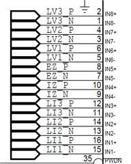
#3 channel : Voltage measurement (3phase)
#3 channel : Current measurement (3phase)
#1 chanel : Internal-zero current measurement.
#1 chanel : External-zero current measurement.

#External Clock Frequency= 2.048 MHz

#Analog ground and digital ground are not split.

# SPI I/F config.  see below

DRDY : 8kHz

Speed: 16MHz

Here is result is the tests about EMC.

Surge Test : 4kV Passed

Burst Test(EFT: IEC 61000-4-4) : 1kV Passed,  2kV Failed.  (Both 5kHz and 100kHz)

<Failed> does not mean that the IC or product is damaged.
It means that the ADC measurement value changes and operates abnormally.

I have a question.

1. The ESD Level (HBM, CDM) is lower than other parts. Can this affect the burst immunity test? 

*ESD voltage of ADC131E08 listed in Datahseet appears to be around 500V.

2. Datasheet says that ground split is not mandantory . Could it be a problem if it is used as a common ground(=not split condition)?

When communicating with the main MCU and ADC IC, a issue occurs with the measured value, If remove the ADC IC you won't have any problems. (=burst tests passed up to 4kV)

but 

The Main MCU is in PCBA-1, and the ADC IC is in PCBA-2. It two pcba are connected by a shielded cable. it call FPCB.

SPI's totally length is 100mm.

I can't find about solution.  Is it conducted noise or radiated noise?

# Reference voltage is 1.65V and a resolution of 24 bits is used.

# PCB is 6 Layers.

TOP (1-Layer) - Placement + signal

IN-1 (2-Layer) - Power plane

IN-2 (3-Layer) - GROUND PLANE

IN-3 (4-Layer) - Signal Layer

IN-4 (5-Layer) - GROUND PLANE

BTM (6-Layer) - Placement + signal

Shuld I additional ESD Coponents? or should I chaged PCB Design? or other things?


  • Hi Daesung,

    Welcome to the E2E forum.

    The purpose of ESD protection on chips is to protect the device from ESD damage during manufacturing and assembly, but it is not intended to design and protect the finished product when it is powered up.

    EMC compliance testing including IEC 61xxx is a system level test. This kind of test is highly related to your PCB board layout design, proper protection design and so on. Definitely you need proper protections for the input, power supplies and interface of your circuit, the protection technique depends on your application, the structure of ADC and so on.

    Your PCB stackup is good even though it is not the best design. A solid ground plane is a better approach as I have seen customers failed EMC testing with their split ground layout design and finally passed after they redesigned with a solid ground plane.

    We have done an EMC compliance test for a reference design with ADS8686 which is a precision SAR ADC, EMC Compliance Testing for Precision ADC Systems. We will release more application reports for EMC compliance testing and design in the future.

    BR,

    Dale

  • Thanks Dale,

    so I have additional question,

    I understood it you told me about it is better to use a "ground plane" rather than a split ground.

    1. it means if using a ground plane, should I use an anti-pad on a PCBA to unuse other layers and go directly to the ground on the 3 layer(ground plane) or 5 layer(ground plane). am I right?

    2. Are there any EMC test results for ADS131E08 other than ADS8686?

    3. is mandantory digital isolators for SPI Interface's storng EMC conditon?

  • Hi Daesung,

    Please see my answers below.

    1. I do not understand what your 'anti-pad on a PCBA' is. A solid ground plane means there is no break in the copper on the inner or top/bottom ground layer, it is just a solid plane. The GND pin of ADC or other components can be directly connected to the solid ground plane through via which provides a short path to the ground plane. A solid ground plane provides some degree of protection against electromagnetic interference (both radiated and received). 

    2. Unfortunately, we did not do EMC test for ADS131E08. As I said, this is a system level test and not a standard for chip test, we are doing such a test for some ADCs for specific applications, but the system design guideline to pass EMC test is same for any device.

    3. The failure could be caused by any circuit or component in your system including the digital communication between the ADC and your microcontroller. The solution of digital isolation+isolated power supply is very helpful to protect the components from electromagnetic interference and pass the test especially for your strong EMC condition, e.g. 100kHz and 2 or 4kV EFT.

    BR,

    Dale

  • Hi Dale ,

    Thanks a lot your information. and I have one last question,

    PCBA is designed as a 6-layer board, and the TOP and BTM are entirely covered with copper. It is designed as a through-hole board rather than a build-up board, so all grounds are connected.

    If you look at my post, the ground plane layers are the 3rd and 5th floors.

    Should I direct the via to the 3rd or 5th floor and then strengthen the 3rd and 5th floors with stitching vias?

    Currently, the ground of all layer is designed with through-hole vias .

    *what I means anti pad of via as here.


    Through-hole vias are used rather than build-ups, but the ANTI PAD is set so that the 1st, 2nd, 4th, and 6th floors are not connected to the ground. This allows you to go directly to the ground plane.

  • Hi Daesung,

    Thanks for your clarification. Yes. Please see the more information in the TI Precision Labs ADC  series - PCB design for good EMC.

    BR,

    Dale