This thread has been locked.

If you have a related question, please click the "Ask a related question" button in the top right corner. The newly created question will be automatically linked to this question.

ADC3642: ADC3642

Part Number: ADC3642

Tool/software:

Hello Again TI support Team,

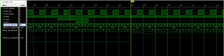
I've been using this ADC in my design for a few months now, and just now noticed an issue that required special attention on signal delay(latency).  When I look at the ADC output, I observed approximately 3-4 clocks of additional delay from where I expected the signal to be.  In the screen capture below, I expected to see the rising edge of da13_0_porta[13:0] after 3.5clks(2.5clks for DDR to SDR conversion + 1clk of latency)  from the rising edge of Usig1 signal.  Instead, it is showing much later.  

My configuration is CMOS DDR with offset binary enabled(Registers -->0x8F=0x02, 0x92=0x02, and 0x24=0x04).   

My set up uses Usig1 signal as trigger which is fed to a FG.  The output of said FG is fixed to a delay of zero between these 2 signals and is fed into a Diff Amp which then feeds the square wave into the ADC.  I just measure the delay on the output of the ADC and it is not what i expected.  Anyways, I'd greately appreciate any feedback that helps me reduce this delay.    

Thanks in advance,

Paulino

  • Hi Paulino,

    Can you let us know what you used for verify this latency initially?

    Was it an EVM from TI or devices you ordered?

    Please advise?

    Pictures of the device used previously and the current devices would help expedite these differences.

    Thanks,

    Rob

  • Hello Rob,

    I used my own board.  The configuration was the default configuration with 2's complement.  In this format I measured the latency to be 1x clk cycle(40ns) as per DS. 

    We then found out 2's complement was not useful in our design and changed the format to binary by programming registers 0x8F and 0x92 (0x8F=0x92=02).  Bit D2 in register 0x24 (0x24=04) was also enabled as recommended in 0x8F and 0x92 (so 0x24=04).  But bit D2(DIG BYP) in 0x24 enables the digital features block which will automatically add delay so I have tried setting D2=0. It does not help.  Is there any other register involved that I might be missing to set minimum latency?  

    Thanks in advance,

    Paulino

  • Hi Paulino,

    Let me look into this more. Can you please send over your register log/writes for the ADC?

    Thanks,

    Rob