This thread has been locked.

If you have a related question, please click the "Ask a related question" button in the top right corner. The newly created question will be automatically linked to this question.

DAC38J82: No waveform output from DAC38J82

Part Number: DAC38J82
Other Parts Discussed in Thread: LMK04828

Tool/software:

Hello, 

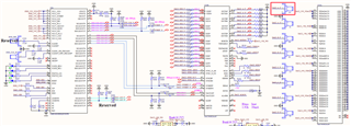
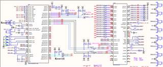
I run a example for DAC38J82 using TI204C-IP.

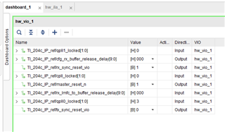
And I got the register value from 0x64 to 0x6C from DAC38J82. Below is the value.

Reg 0x64 = 0

Reg 0x65 = 0

Reg 0x66 = 0

Reg 0x67 = 0

Reg 0x68 = 0

Reg 0x69 = 0

Reg 0x6A = 0

Reg 0x6B = 0

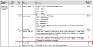
Reg 0x6C = 0x3 ( Bypass DAC PLL)

So I have 2 questions.

Question1: From DataSheet, Reg 0x6C bit1 is reserved and should be 0, but I got 1. Is it normal?

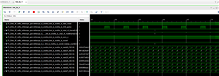
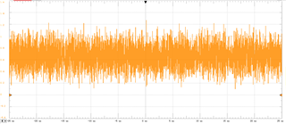
Question2: From the register value, It seems DAC working normal, after pull up TXEN, but I cannot see waveform from output A+. Is it any other possiable?


Thanks

Best regards

Daniel

  • Hi Daniel,

    Can you please send us your schematic of the DAC and output frontend? Let us know where you are probing as well.

    Thanks,

    Rob

  • Hi Bob,

    Below is my schematic about DAC38J82, and I connect A+ to scope directly. 

    Thanks

    Best regards

    Daniel

  • Daniel,

    Can you try writing 0x03 bit 0 as 1 to set the sif_txenable? Please provide full register configuration sequence for the DAC for further help. What is the sample rate? You are using the TI204C-IP? Is RX lane width 32 bit or 64 bit?

    Thanks, Chase

  • Hi Chase,

    I have try writing 0x03 bit 0 as 1, same result. 

    Attached is my steps for DAC38J82.

    First, execute DAC38J82_Setup(), then DAC38J82_ResetJESD(), then DAC38J82_ReadStatus().

    My target sample rate is 312.5M, 8 lane, interp x1.

    DACCLK input is 312.5M, JESD lane rate is 1.5625G.

    Using TI204C-IP V1.12, TX_LANE_DATA_WIDTH = 64

    Thanks

    Best regards

    Daniel

    DAC38J82_Setup()
    {
    
    	write reg 0x00 = 0x0018
    	write reg 0x01 = 0x0003
    	write reg 0x02 = 0x2082
    	write reg 0x03 = 0xA300
    	write reg 0x04 = 0x0000
    	write reg 0x05 = 0xFF03
    	write reg 0x06 = 0xFFFF
    	write reg 0x07 = 0x3100
    	write reg 0x08 = 0x0000
    	write reg 0x09 = 0x0000
    	write reg 0x0A = 0x0000
    	write reg 0x0B = 0x0000
    	write reg 0x0C = 0x0400
    	write reg 0x0D = 0x0400
    	write reg 0x0E = 0x0400
    	write reg 0x0F = 0x0400
    	write reg 0x10 = 0x0000
    	write reg 0x11 = 0x0000
    	write reg 0x12 = 0x0000
    	write reg 0x13 = 0x0000
    	write reg 0x14 = 0x0000
    	write reg 0x15 = 0x0000
    	write reg 0x16 = 0x0000
    	write reg 0x17 = 0x0000
    	write reg 0x18 = 0x0000
    	write reg 0x19 = 0x0000
    	write reg 0x1A = 0x0023
    	write reg 0x1B = 0x0000
    	write reg 0x1E = 0x9999
    	write reg 0x1F = 0x9980
    	write reg 0x20 = 0x8008
    	write reg 0x22 = 0x1B1B
    	write reg 0x23 = 0x01FF
    	write reg 0x24 = 0x0020
    	write reg 0x25 = 0x4000
    	write reg 0x26 = 0x0000
    	write reg 0x2D = 0x0001
    	write reg 0x2E = 0xFFFF
    	write reg 0x2F = 0x0004
    	write reg 0x30 = 0x0000
    	write reg 0x31 = 0x1000
    	write reg 0x32 = 0x0000
    	write reg 0x33 = 0x0000
    	write reg 0x34 = 0x0000
    	write reg 0x3B = 0x0000
    	write reg 0x3C = 0x0228
    	write reg 0x3D = 0x0088
    	write reg 0x3E = 0x0148
    	write reg 0x3F = 0x0000
    	write reg 0x46 = 0x0044
    	write reg 0x47 = 0x190A
    	write reg 0x48 = 0x31C3
    	write reg 0x49 = 0x0000
    	write reg 0x4A = 0xFF3E
    	write reg 0x4B = 0x1200
    	write reg 0x4C = 0x1F07
    	write reg 0x4D = 0x0101
    	write reg 0x4E = 0x0F4F
    	write reg 0x4F = 0x1C61
    	write reg 0x50 = 0x0000
    	write reg 0x51 = 0x00DC
    	write reg 0x52 = 0x00FF
    	write reg 0x53 = 0x0000
    	write reg 0x54 = 0x00FC
    	write reg 0x55 = 0x00FF
    	write reg 0x56 = 0x0000
    	write reg 0x57 = 0x00FF
    	write reg 0x58 = 0x00FF
    	write reg 0x59 = 0x0000
    	write reg 0x5A = 0x00FF
    	write reg 0x5B = 0x00FF
    	write reg 0x5C = 0x1133
    	write reg 0x5E = 0x0000
    	write reg 0x5F = 0x0123
    	write reg 0x60 = 0x4567
    	write reg 0x61 = 0x0211
    	write reg 0x64 = 0x0001
    	write reg 0x65 = 0x0001
    	write reg 0x66 = 0x0001
    	write reg 0x67 = 0x0001
    	write reg 0x68 = 0x7709
    	write reg 0x69 = 0x0000
    	write reg 0x6A = 0x0000
    	write reg 0x6B = 0xBD07
    	write reg 0x6C = 0x0007
    	write reg 0x6D = 0x0090
    	write reg 0x6E = 0x0000
    	write reg 0x6F = 0x0000
    	write reg 0x70 = 0x0000
    	write reg 0x71 = 0x0000
    	write reg 0x72 = 0x0000
    	write reg 0x73 = 0x0000
    	write reg 0x74 = 0x0000
    	write reg 0x75 = 0x0000
    	write reg 0x76 = 0x0000
    	write reg 0x77 = 0x0000
    	write reg 0x78 = 0x0000
    	write reg 0x79 = 0x0000
    	write reg 0x7A = 0x0000
    	write reg 0x7B = 0x0000
    	write reg 0x7C = 0x0000
    	write reg 0x7D = 0x0000
    
    }
    
    DAC38J82_ResetJESD()
    {
    	write reg 0x4A = 0xFF30
    	write reg 0x4A = 0xFF3E
    	write reg 0x4A = 0xFF3F
    	write reg 0x4A = 0xFF31
    
    	write reg 0x03 = 0xA301
    
    }
    
    DAC38J82_ReadStatus()
    {
    	//Clear
    	write reg 0x41 = 0x0000
    	write reg 0x42 = 0x0000
    	write reg 0x43 = 0x0000
    	write reg 0x44 = 0x0000
    	write reg 0x64 = 0x0000
    	write reg 0x65 = 0x0000
    	write reg 0x66 = 0x0000
    	write reg 0x67 = 0x0000
    	write reg 0x68 = 0x0000
    	write reg 0x69 = 0x0000
    	write reg 0x6A = 0x0000
    	write reg 0x6B = 0x0000
    	write reg 0x6C = 0x0000
    
    	Sleep(100);
    
    	read reg 0x41 is 0x0000
    	read reg 0x42 is 0x0000
    	read reg 0x43 is 0x0000
    	read reg 0x44 is 0x0000
    	read reg 0x64 is 0x0000
    	read reg 0x65 is 0x0000
    	read reg 0x66 is 0x0000
    	read reg 0x67 is 0x0000
    	read reg 0x68 is 0x0000
    	read reg 0x69 is 0x0000
    	read reg 0x6A is 0x0000
    	read reg 0x6B is 0x0000
    	read reg 0x6C is 0x0003
    	
    }
    

  • Hi Chase,

    Do you have any suggestion for this?

    Thanks

    Best regards

    Daniel

  • Daniel,

    I am looking at this today. Stay tuned.

    Thanks, Chase

  • Hi Daniel,

    The main DAC configuration looks fine. I just tested on EVM in this 312.5MSPS mode, 841, and compared register sequence with you. The only changes you have vs my working sequence are related to lane muxing, different K value, lane ID, and using 4w vs 3w spi.

    After the DAC JESD reset is toggled, are you providing at least 2 SYSREF pulses to the DAC? That is the only thing here that will prevent any kind of output from the DAC side. If the lane muxing is incorrect, the output data will just not look correct, but there will be something at least.

    Thanks, Chase

  • Also, your K value is being set to 32 (0x4C 0x1F07) but you're leaving the RBD value as 19 (0x4B 0x1200). You might can try to increase RBD value to 32 by setting 0x4B 0x1F00. I don't think this will solve it because the DAC would be giving elastic buffer overflow errors if that was the case.

    Also, 0x6C reading back as 0x0003 is ok.

    What is the reference clock into the TI JESD IP? For RX lane width of 64 bits, sys clock should be serdes/80 -> 1562.5M/80 = 19.53125MHz. Can you share what the ILA looks like for the TI JESD204? Is master_reset being deasserted while tx_reset is still asserted? After master_reset is deasserted, does the pll lock status report back as 0x3 (since this is 8 lane mode, then 2 quads have to be locked, ie 2b'11 is read back)? Then you can deassert the tx reset.

    Is this all correct?

    Thanks, Chase

  • Hi Chase,

    Thank you for investigation.

    1. I have change RBD to 32, but it is still same result.

    2. "What is the reference clock into the TI JESD IP?" . I only have TX in TI JESD IP, the tx_sys_ref not used and tie 0 in example design.

    3. Also I have try continues SYSREF for DAC. Still not work.

    4. The qpll_locked is 2'b11, please see attached screenshot. I also attached my schematic and LMK04828 settings, please help see any issue.

    5. About muxing, do you mean the SERDES lane to JESD lane muxing? As my understanding, usually it will be One-to-one correspondence (SERDES lane0 to JESD lane0, SERDES lane1 to JESD lane1, etc.). Is it correct ?

    6. May I know the sequence about reset. Reset DAC JESD first or reset TI JESD204 first ?

    7. Would you please share your DAC38J82 settings?

    Thanks

    Daniel

    LMK04828_Setup()
    {
    
    	//Input 312.5M
    	write_reg  0x0000 = 0x80
    	write_reg  0x0000 = 0x10 //Set SPI 4 wire
    	write_reg  0x014A = 0x33
    	write_reg  0x0002 = 0x00
    	write_reg  0x0100 = 0x02
    	write_reg  0x0101 = 0x55
    	write_reg  0x0103 = 0x00
    	write_reg  0x0104 = 0x20
    	write_reg  0x0105 = 0x00
    	write_reg  0x0106 = 0xF0
    	write_reg  0x0107 = 0x11
    	write_reg  0x0108 = 0x61
    	write_reg  0x0109 = 0x55
    	write_reg  0x010B = 0x01
    	write_reg  0x010C = 0x20
    	write_reg  0x010D = 0x00
    	write_reg  0x010E = 0xF0
    	write_reg  0x010F = 0x76
    	write_reg  0x0110 = 0x08
    	write_reg  0x0111 = 0x55
    	write_reg  0x0113 = 0x00
    	write_reg  0x0114 = 0x00
    	write_reg  0x0115 = 0x00
    	write_reg  0x0116 = 0xF9
    	write_reg  0x0117 = 0x00
    	write_reg  0x0118 = 0x18
    	write_reg  0x0119 = 0x55
    	write_reg  0x011B = 0x00
    	write_reg  0x011C = 0x20
    	write_reg  0x011D = 0x00
    	write_reg  0x011E = 0xF9
    	write_reg  0x011F = 0x00
    	write_reg  0x0120 = 0x10
    	write_reg  0x0121 = 0x55
    	write_reg  0x0123 = 0x00
    	write_reg  0x0124 = 0x00
    	write_reg  0x0125 = 0x00
    	write_reg  0x0126 = 0xF9
    	write_reg  0x0127 = 0x11
    	write_reg  0x0128 = 0x08
    	write_reg  0x0129 = 0x55
    	write_reg  0x012B = 0x00
    	write_reg  0x012C = 0x00
    	write_reg  0x012D = 0x00
    	write_reg  0x012E = 0xF9
    	write_reg  0x012F = 0x00
    	write_reg  0x0130 = 0x08
    	write_reg  0x0131 = 0x55
    	write_reg  0x0133 = 0x00
    	write_reg  0x0134 = 0x20
    	write_reg  0x0135 = 0x00
    	write_reg  0x0136 = 0xF9
    	write_reg  0x0137 = 0x01
    	write_reg  0x0138 = 0x40
    	write_reg  0x0139 = 0x03 //continues sys ref
    	write_reg  0x013A = 0x00 //sys ref 19.53M
    	write_reg  0x013B = 0x10 //sys ref 19.53M
    	write_reg  0x013C = 0x00
    	write_reg  0x013D = 0x08
    	write_reg  0x013E = 0x03
    	write_reg  0x013F = 0x00
    	write_reg  0x0140 = 0x00
    	write_reg  0x0141 = 0x00
    	write_reg  0x0142 = 0x00
    	write_reg  0x0143 = 0x10
    	write_reg  0x0144 = 0xFF
    	write_reg  0x0145 = 0x00
    	write_reg  0x0146 = 0x10
    	write_reg  0x0147 = 0x12
    	write_reg  0x0148 = 0x02
    	write_reg  0x0149 = 0x42
    	write_reg  0x014A = 0x02
    	write_reg  0x014B = 0x16
    	write_reg  0x014C = 0x00
    	write_reg  0x014D = 0x00
    	write_reg  0x014E = 0xC0
    	write_reg  0x014F = 0x7F
    	write_reg  0x0150 = 0x03
    	write_reg  0x0151 = 0x02
    	write_reg  0x0152 = 0x00
    	write_reg  0x0153 = 0x00
    	write_reg  0x0154 = 0x78
    	write_reg  0x0155 = 0x00
    	write_reg  0x0156 = 0x78
    	write_reg  0x0157 = 0x00
    	write_reg  0x0158 = 0x96
    	write_reg  0x0159 = 0x00
    	write_reg  0x015A = 0x78
    	write_reg  0x015B = 0xF4
    	write_reg  0x015C = 0x20
    	write_reg  0x015D = 0x00
    	write_reg  0x015E = 0x00
    	write_reg  0x015F = 0x0B
    	write_reg  0x0160 = 0x00
    	write_reg  0x0161 = 0x01
    	write_reg  0x0162 = 0x44
    	write_reg  0x0163 = 0x00
    	write_reg  0x0164 = 0x00
    	write_reg  0x0165 = 0x0C
    	write_reg  0x0166 = 0x00
    	write_reg  0x0167 = 0x00
    	write_reg  0x0168 = 0x0C
    	write_reg  0x0169 = 0x5B
    	write_reg  0x016A = 0x20
    	write_reg  0x016B = 0x00
    	write_reg  0x016C = 0x00
    	write_reg  0x016D = 0x00
    	write_reg  0x016E = 0x13
    	write_reg  0x017C = 0x15
    	write_reg  0x017D = 0x0F
    
    	Sleep(50);
    }
    

  • Hi Daniel,

    If the pll is locking on FPGA side, the reference clock will be correct.

    When I say lane muxing I am referring to the muxing to correct for any mismatch between the FPGA output lane and the DAC input lane. I'm not familiar with the mapping on your hardware so for now it is ok. This won't prevent any output from showing - if incorrect it would just look badly.

    The sequence for bringup is:

    1. Configure LMK
    2. Assert DAC reset (should be hardware reset but I tested and can confirm software reset is ok (assert register 0x02 bit 0)
    3. Configure DAC
    4. Assert master reset
    5. Assert tx reset
    6. Deassert master reset
    7. Verify PLL locks
    8. Deassert tx reset (after deasserting tx reset, FPGA will start transmitting data over serdes, whether K28.5 symbols or data depending on SYNCb state)
    9. Toggle DAC JESD Reset
    10. Assert 2 SYSREF pulses to DAC (automatic if using continuous sysref)

    Full settings here: 

    evm_config_works.cfg

    I notice the SYSREF input to the DAC says LVDS but you are terminating it as if it was LVPECL through 200Ω pulldowns and then AC coupling, all while the LMK output format for SDCLKOUT3 is set as LCPECL. For an AC coupled LVDS output of the LMK04828, there should be a light 560Ω differential termination before series AC caps. Can you try changing the output format for the SDCLKOUT3 output to LVPECL1600mV by changing register 0x10F to 0x56 instead of 0x76?

    Thanks, Chase

  • Hi Chase,

    I have try the  output format for the SDCLKOUT3 output to LVPECL1600mV, still not work.

    Also I have check the lane mapping from FPGA to DAC. My understand is if the mapping is wrong, the ILAs will mismatch for LaneID between JESD IP and DAC reg config, and the link cannot be established. Is it right?

    Attached is my waveform now, seems noise.

    I will check everything again.

    Thanks, Daniel

  • Daniel,

    If the Lane ID does not match then the DAC will give a link configuration error. You can try toggling the mem_no_lane_sync field (register 0x4F bit 5) which will ignore the link configuration errors.

    Thanks, Chase