Tool/software:
1)
Does note 3, under 6.1, mean that vin can exceed the absolute maximum voltage of VA + .300 or go below -.300V provided the pin current is limited to less than +-10mA and total current less than +/-20ma?
Or does note 3, under 6.1 mean the current on an input pin must be less than +/-10mA if the pin voltage exceeds the operating voltage (0V to Va), but Vin must still always be in the range of the absolute max voltages of -0.3V to Va+0.3V to prevent damage?
2)
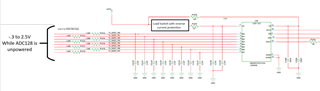
As shown in the attached schematic fragment we can have voltages between -0.3V to 2.5V present on the Vin pins while the 5962R0722701VZA is unpowered. These voltages will cause current to flow through the ESD diodes sourcing current out of the Va pin. Our approach to mitigate the detrimental impact on upstream circuits is to isolate the Va pin using a load switch with reverse current protection as shown in the attached. Is it possible for the resulting voltage on the Va pin to cause anomalous behavior or prevent the adc from powering up and operating correctly once the load switch is turned on and the adc is finally powered?