This thread has been locked.

If you have a related question, please click the "Ask a related question" button in the top right corner. The newly created question will be automatically linked to this question.

Reg. Analog Input Protection for ADS8364

Other Parts Discussed in Thread: ADS8364

Hello,
I am using the Analog to Digital Converter IC ADS8364 in my board.
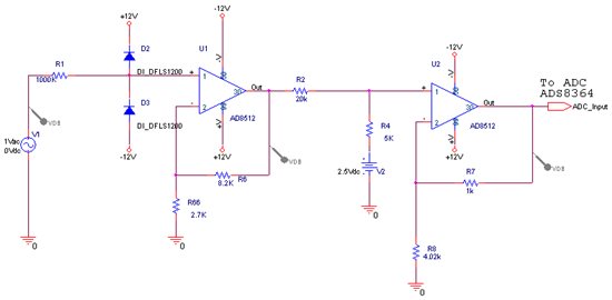
A sensor output is signal processed by an opamp and fed to the input channel of AD8364 in single ended mode. (CHx negative connected to +2.5V)
At times, there are good probabilities that the input to the ADC may go beyond +5V and below 0V at CHx +.
I could see that the ADC input is having a voltage clamping scheme internally.
Please let me know if the ADC can withstand continuous voltages from +11V to -11V (opamp saturation voltage).
I tried clamping the ADC input with a Zener, but it has exponential characteristics near breakdown region and is unfit for accurate measurement purposes.

To limit the power dissipation in the internal clamping diodes, I can connect a resistor in series to the opamp output and ADC input.
If, by connecting a series resistor the ADC can tolerate +11V to -11V, please suggest the series resistor value.
Since the board is already fabricated, I am unable to connect those clamping rectifier diodes externally.

Thanks and Regards,
Mohmed Anees

  • Hi!

    What does the opamp do? Things would get much easier if the opamp uses the same supply voltage as your adc.
    Can you insert a resistor between the opamp-output and the adc-input to limit the clamping current (or do you have fast, dynamic signals)?

    Regards,
    Edwin Krasser

  • Hi,

    The opamp is used to signal condition a sensor ouput (Add an offset voltage of 2.5V and multiply with a factor of 2, filter out frequencies above 32Khz at -3db).

    I can connect a series resistor at the opamp output  and ADC input. But I am not sure whether with this series resistor would enable the ADC to tolerate +/-11V continously.

    If yes, how much should be the series resistor value as it should not affect the ADC reading and at the same time protect the ADC internal clamping diodes. I would also want to know the wattage of the internal protection diode used, so that the series resistor value can be chosen.


    Thanks,

    Anees

  • Hi,

    if I understand correctly, you do some level conversion (bipolar signal to a 0-5V-Signal: +2.5V), amplification by the factor of 2 and low pass filtering (first order? second order sallen key or multiple feedback topology?)
    There exists a nice solution using one opamp and some resistors for this application (R2=2*R1 => gain=-2, inverting amplification should not be a problem):


                ------R2-------

                |             |

                |  +5V        |

                |   |         |

    x ------R1--o---| - \     |

                    |     \ --|----out (0..5V)

    Vref ---R3--o---| +   /

                |   |   /

               R4   |

                |   |

               GND GND

    Calculation of R3/R4: Vref*R4/(R3+R4)*(1+R2/R1)=2.5 => Vref*R4/(R3+R4)=2.5/3
    If you have the 2.5V for Vref => R4/(R3+R4)=1/3 => R3=2*R4

    Moreover, because at the noninverting input is just a dc signal, you can filter it with a capacitor (parallel to R4) and, if you need this level shifting more than once, you will need the R3/R4 (& capacitor) just once. The opamp cannot output more than 5V (adc is safe). But now the input clamping diodes of the opamp inverting input must be able to survive the clamping current when x gets out of the limits. E.g. if x is -5V and R1=10k, R2=20k there will be a clamping diode current of 5/10k=0.5 mA. Check the opamp datasheet, but clamping currents below 1 mA should not be a problem (for most parts). If it's too much or the input impedance is too small, just use a greater R1 value (e.g. 100 kOhm).
    And one more thing: If you want to get a first order low pass filter, just add a capacitor in parallel to R2 ( fc=1/(2*pi*R2*C) ).

    Best regards,
    Edwin Krasser

  •  

    Hi,

    I am using a dual supply opamp and hence connected the supplies to +5V & -5V.

    Vref is connected to 2.5V. R3 = 2K & R4 = 1K.

    Source V1 is kept in DC Sweep mode swinging from -5V to +5V.

    The simulated output is shown below.


    As per the requirement, I need

    Input        Output

    -2.5V         0V

    0V              +2.5V

    +2.5V        +5V

    Moreover, as per the proposed solution if the opamp is connected is single supply mode, we cannot give positive voltages to the inverting pin. But the input voltage is bipolar.

    Please let me know if i could clarify anything further.


    Thanks,

    Anees

  • Hi,

    First of all, I recommend to use GND and +5V as opamp supply (opamp with rail to rail output). Hence, you cannot get negative output voltages which might harm the adc inputs.

    As long the feedback is working (vin: -1.25 to +1.25), the common mode voltage will be constantly 2.5/3 = approx. 0.83 V. Positive or negative input voltages do not matter. But, if you leave the input voltage range of -1.25 to +1.25 V, the output of the opamp will keep at its supply limit (0 or +5V). And only in this case, the voltage at the inverting input will change (because the feedback does not work any more) and might try to leave the supply voltage range (=> clamping diodes).

    Best regards,
    Edwin Krasser

    Here is my LTspice dc simulation result (green: output voltage, blue: voltage at inverting opamp input, D1,D2 simulate the clamping diodes):

  • Hi,

    Thanks for your simulation results.

    Based on the simulation results,

    IP                  OP

    -1.25V         +5V

    0V                +2.5V

    +1.25V        0V


    Requirement:

    IP               OP

    -2.5V          0V

    0V               +2.5V

    +2.5V       +5V (Sorry, Input wrongly mentioned as +1.25V in my previous post)

    With the schematics as shown in the attachment, the requirement as above is realized.

    The issue here is, limiting the opamp output (U2) to 0 to +5V.

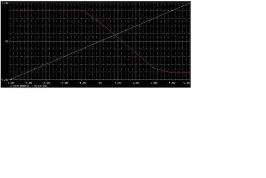
    Note: Since the board is already fabricated, it is very difficult to have flexibility in the voltage supplies. I Planned to use a zener at the output of U2 (which is the input to ADC), so that it gets clamped at +5.1V and -0.3V (which is safe). But, near zener breakdown area, the curve gets exponential and makes it unfit for measurement purposes.

    If you can share your contact number, I can talk to you at your convenient time and explain more on this.

  • Hi!

    Well, gain is 1. So you just want to shift +/- 2.5V to 0-5V. Ok. If your boards are already fabricated and real modifications can be done in the next redesign (which should be done), I will suggest to use a larger resistance value for R2. So that the complete possible input range will be mapped to 0-5V => +/- 12V to 0-5V, gain=5/24 approx 0.2 (instead of 1). R2 should be about 40 kOhm (and reduce the gain of your second opamp to 1 => no 10k resistor to ground). Ok, you will lose 2.3 bit in the digital resolution but you will not have problems with the adc input range. It's a tradeoff, not a good one but it should help.

    Best regards,
    Edwin Krasser

  • Hi,

    The circuit is modified as shown above for over voltage protection.

    since the opamp input will experience high voltages (300V), this circuit will give a continuous protection to ADC.

    +2.5 to -2.5 input is mapped to +10/-10V at the first opamp (Saturation) and offset is added by 2.5V.

    Second opamp gain is 1.25, thereby +2.5V to -2.5V will produce +5V to 0V at the ADC inputs and provide continuous over voltage protection to the ADCs.

    Your ideas have helped me a lot in arriving at this configuration. Please let me know if you see any problems with this circuit. It is working in simulation as expected.

    Thanks,

    Anees