This thread has been locked.

If you have a related question, please click the "Ask a related question" button in the top right corner. The newly created question will be automatically linked to this question.

ADC3669: Programming sequence

Part Number: ADC3669

Tool/software:

Hello

We designed prototype board with new ADC 3669 and with Altera ArriaV FPGA. We already implemented the communication with ADC and compiled appropriate deserialization in FPGA. We try to correctly set registers in ADC which we need for our application (dual channel, dual DDC with complex decimation by 4). We believe that we configure all necessary registers, but we cannot find the reliable programming sequence for stable ADC function. We must randomly configure registers  0x167/168/168 with specific content to get working state. There is not so many application examples regarding the programming sequence at TI web sites. Can we get a support for ADC3669 and resolve this issue?

Josef

  • Hi Josef,

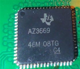
    I can certainly help you with the configuration of the ADC3669. First, can we confirm whether you have pre-production samples or production silicon? If you could send a picture of the device itself with the markings on the chip clearly visible, I can confirm.

    Best,

    Luke Allen

  • HI Luke

    attached is picture of device package.

    Josef

  • Hi Josef,

    Great, looks like you have production silicon. Thank you for confirming.

    Before bringing up the ADC, please ensure that you are supplying a clock and apply a hardware reset pulse (active high).

    You can use the following sequence to program the ADC for Dual Channel, Dual DDC, Complex Decimation by 4:

    # Setup mode
    write(0x100,0x1) # Software Reset
    write(0x169,0x2) # Common Decimation Factor set to 4
    write(0x162,0x4) # Enable Complex Decimation
    write(0x169,0x12) # Set to Dual DDC Mode

    # Set NCO Freqs
    # DDC0, NCOFreq0 set to 69MHz
    write(0x200,0x16)
    write(0x201,0xd9)
    write(0x202,0xce)
    write(0x203,0xf7)
    write(0x204,0x53)
    write(0x205,0x23)
    # DDC1, NCOFreq0 set to 70MHz
    write(0x240,0xa3)
    write(0x241,0x70)
    write(0x242,0x3d)
    write(0x243,0xa)
    write(0x244,0xd7)
    write(0x245,0x23)

    # Update and Synchronize
    write(0x165,0x1) # Update NCO Frequencies (on 0 - 1 transition)
    sleep(0.001) # Wait for 1ms
    write(0x165,0x0) # (set back to zero)
    write(0x161,0x82) # Mask Timer and LVDS block so sysref pulse only goes to DDC and NCO
    write(0x160,0x3) # Pulse Sysref (to synchronize DDCs on 0 - 1 transition)
    sleep(0.001) # Wait for 1ms
    write(0x160,0x0) # (set back to zero)

    I used the example of an NCO frequency of 69MHz for DDC0 (CHA by default) and a NCO frequency of 70MHz on DDC1 (CHB by default). You can make any changes needed for you application, but this should reliably configure the ADC into your desired mode.

    Best,

    Luke Allen