This thread has been locked.

If you have a related question, please click the "Ask a related question" button in the top right corner. The newly created question will be automatically linked to this question.

No signal from the DOUT pin in ADS1299 EEG-FE

Other Parts Discussed in Thread: ADS1299, CC2540

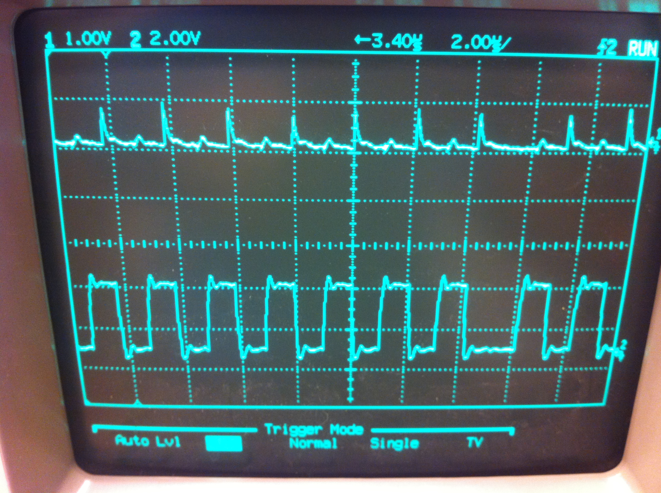
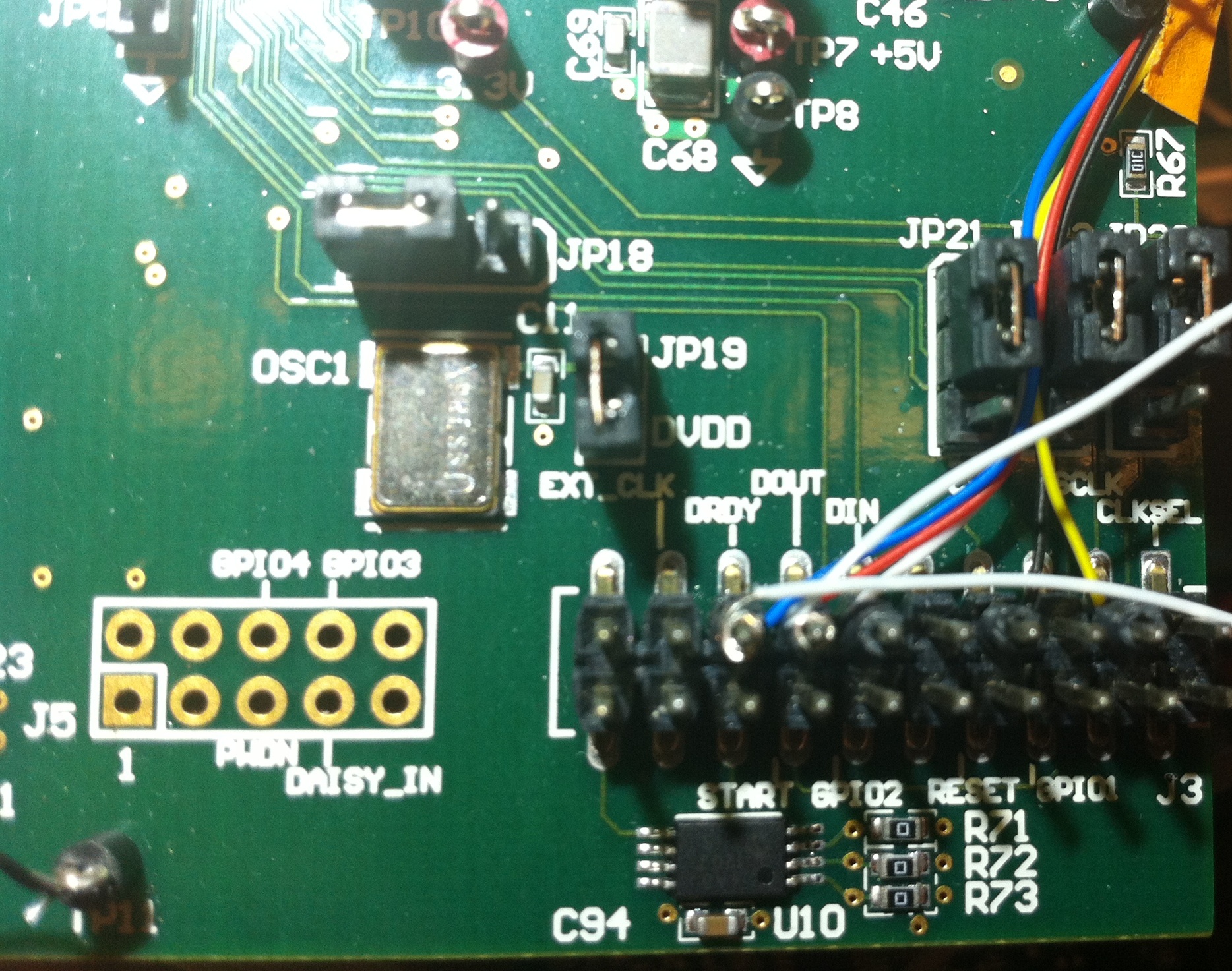
I am trying to read data from DOUT pin in the ADS1299 EEG-FE without the MMB0 board. I have sent a SCLK clock (bottom of the figure) of 8 bits *27 using a 8-bit MCU.  The default read data mode of the ADS1299 is RDATAC, right? I can detect correct DRDY_bar and CS_bar signals. But I cannot get signals from the DOUT (above of the figure) if I connect the CH1 with a signal source.

Is it because I am reading the buffer in a byte-by-byte other than 24-bit way? I noticed there is a half T_sclk dalay when a 8 -bit clock is generated. Does it matter?

Or I should configure some registers of ADS1299 first so that it can send data?

Thank you for some advices.


  • Hi Xinling, 

    Yes, the default mode for reading back data is RDATAC. The way you describe reading the data should be fine. The only concern with an SCLK that is too slow (with too much delay between 8-bit bursts) is that you may not finish reading all of your 8-channel data before the next /DRDY.

    The MMBO is used to provide both power supplies as well as the SPI communication signals. Can you please confirm that these signals are being routed properly to the ADS1299? Check to make sure that you have JP21 and JP23 configured correctly on the ADS1299 daughterboard and that you are probing /CS, /DOUT, and SCLK on the appropriate J3 pins.

    Regards,

  • Hi, Ryan, Thank you so much for your reply.

    I am using a SCLK boud rate of 480.5kHz and the default data rate of ADS1299 EEG-FE is 250 SPS, is the SCLK too slow?

    JP21,JP22,JP23 are all connected by 1-2 as factory default. I am probing /CS from pin 7 of J3, /DOUT from pin 13 of J3, and SCLK from pin 3 of J3.  When I use MMB0 to communicate with ADS1299 EEG-FE, I can get correct signals using the ADS1299 EEG-FE software, so I think the jumper and signal are configured correctly.  

    I am thinking there might be some errors in my SPI read program. Will you please take some time to have a look at it? Thank you.

    while (DRDY == 0)

         {

          // Clear SSN, the SPI slave is active when SSN is low.

          CS = CS_ENABLED;

          int i;

          for (i = 0; i< 27; i++)   //27 bytes to read

          {

            // Clear transmit byte status.

            U1CSR &= ~0x02;   

            // Write dummy byte to USART1 buffer to trigger SCLK.

            U1DBUF = dummyByte;     

            // Check if byte is transmitted (and a byte is recieved).

            while(!(U1CSR & 0x02));

           // Write received byte to buffer.

            rxBufferMaster[i] = U1DBUF;

           }

           // Set SSN, the SPI slave is inactive when SSN is high.

            CS = CS_DISABLED;

         }

    BTW, how can I read and write registers of ADS1299? For example, if I want to send the command SDATAC to stop the RDATAC mode and change the data rate in CONFIG1 register to 1000 SPS, should I just write 0x11(SDATAC) to the buffer?  Is the code below right?

    while(1)

    {

    CS = CS_ENABLED;

    U1CSR &= ~0x02; // Clear transmit byte status.
    U1DBUF = 0x11;  // Write SDATAC(11h) to stop RDATAC mode.
    while(!(U1CSR & 0x02)); // Check if byte is transmitted (and a byte is recieved).


    // write CONFIG1 to change date rate to 500 SPS.

    U1CSR &= ~0x02; 
    U1DBUF = 0x41;   // WREG Opcode 1---- CONFIG1 address: 01H
    while(!(U1CSR & 0x02)); 

    U1CSR &= ~0x02; 
    U1DBUF = 0x00;  // WREG Opcode 2---- No. of register: 1

    while(!(U1CSR & 0x02)); 


    U1CSR &= ~0x02; 
    U1DBUF = 0x94;  // Data rate of 1000 SPS

    while(!(U1CSR & 0x02)); 


    CS = CS_DISABLED;

    }

  • Hi Xinling, 

    Your SCLK speed is ok. The minimum requirement for eight 24-bit channels + STATUS at 250 SPS is 55 kHz as calculated by Equation 6 on page 26 of the datasheet.

    If JP21 = [1-2], /CS is tied to J3 pin 1, not pin 7.

    If JP22 = [1-2], your START signal is tied to /CS. Default for JP22 is [2-3] so that START is tied to J3 pin 14.

    If JP23 = [1-2], then CLKSEL is tied to GND and you must provide an external clock. 

    Please confirm that you are using the correct jumper settings for /CS, START, and CLKSEL.

    Thanks and regards,

  • Hi, Ryan,

    Thank you so much for your reply. I really really appreciate your detailed instructions.

    I know from the diagram in page 53 of the EEG-FE user guide that all JP21-23 should be set to 1-2. However, when I tried to use this configuration, I cannot get the correct DRDY, CS and SCLK signal. The CS in pin 1 would be 3.2 V no matter the program drops it to zero.  Besides, the factory default setting is connecting pin 2-3 of JP21-23 for my board (ADS1299 EEG FE Rev A), and I can use this setting to record correct signals using the MMB0 board.

    If I continue using this setting of my board(that is, DRDY, CS, SCLK and DOUT in pin 15, 7, 3, 13 of J3 respectively, see first figure), I have got the time sequences of DRDY, CS, SCLK and DOUT(bottom figure).

    The first 3 signals (I mean, SPI_DRDY, SPI_CS, SPI_CLK in J3, no matter how I set the JP21-23) are correct, right?

    I cannot get a correct output from DOUT. The amplitude of DOUT trace is about 100 mV, having a negative pulse when the DRDY is negative.

    Besides, whether the START signal in pin 14 of J3 is tied to +3.3V or not, it doesn't influence the time sequences of the four signals. I think that is because the default RDATAC mode has been started, right? Because I can see the period of DRDY signal is 4 ms, corresponding to the default 250 SPS data rate.

    Can you help to tell me what's wrong in my setting?  Thank you very much.

  • The ADS1299 EVM is set up to use one of two possible signals from the MMB0 as the SPI_CS: pin 1 (CNTL) and pin 7 (FSX). These pins are controlled by the MMB0’s TMS320 DSP. In your PCB image, it looks like you have a black wire (I assume /CS from your motherboard) going to J3 pin 7. Since you are not using the MMB0, JP21 needs to be [2-3] to connect /CS from J3 pin 7 to the ADS1299. /DRDY and SPI_CLK will always be tied to J3 pins 15 and 3, respectively.

    Once you send the START opcode to begin conversions, the modulator will continue converting until you tell it to STOP, whether or not you read the data. RDATAC mode allows you to read data each time /DRDY goes low without having to issue the “read” command again and again. You can tie START (J3 pin 14) high to DVDD with 10k resistor and configure JP22 as [2-3] to use this continuous conversion method.

    I have other concerns with the signals shown in the oscilloscope capture. First, each signal appears to be a different amplitude. Please ensure that your GND is shared between your motherboard and the ADS1299 EVM. The digital signals from your processor need to be referred to the same voltage potential as those from the ADS1299. The MMB0 uses level shifters to ensure proper communication between the DSP and the ADS1299.

    Second, it looks like you have a lot of digital feed through from both /DRDY and SCLK. I’m not sure what the cause of this is, so I would start by first correcting your jumper settings and making sure that power and ground is properly shared with your board.

    I’ve attached a schematic of the MMB0 for your reference. 1460.MMB0_Sch_RevD.PDF

  • Hi, Ryan,

    Thank you so much for your timely reply. I learned a lot.

    Yes, there is a black wire tied to pin 7 of J3 as a /CS sending from the motherboard (TI CC2540). Now I know the configuration of these four signals are right. Thank you.

    Do you mean I have to send the START opcode when I power on the ADS1299 EEG-FE? I had thought the chip must have been started working in a RDATAC mode since I can record DRDY signals every 4 ms, which corresponds to the default data rate of 250 SPS.

    I did not send the START opcode because I am not very confident with the write register programs I used.  For example, if I want to send the command SDATAC to stop the RDATAC mode and change the data rate in CONFIG1 register to 1000 SPS, should I just write 0x11(SDATAC) to the buffer?  Is the code below correct?

    while(1)

    { CS = CS_ENABLED;

     U1CSR &= ~0x02;            // Clear transmit byte status.

    U1DBUF = 0x11;              // Write SDATAC(11h) to stop RDATAC mode.
    while(!(U1CSR & 0x02)); // Check if byte is transmitted (and a byte is recieved).

      // write CONFIG1 to change date rate to 500 SPS.

    U1CSR &= ~0x02; 
    U1DBUF = 0x41;             // WREG Opcode 1---- CONFIG1 address: 01H
    while(!(U1CSR & 0x02)); 

     U1CSR &= ~0x02; 

    U1DBUF = 0x00;             // WREG Opcode 2---- No. of register: 1

    while(!(U1CSR & 0x02)); 

      U1CSR &= ~0x02; 

    U1DBUF = 0x94;             // Data rate of 1000 SPS

    while(!(U1CSR & 0x02)); 

     CS = CS_DISABLED;  }

     I am sorry for not explaining the amplitude problem of the oscilloscope capture. I should have done that in my last post to save your time.

    I am using a very old oscilloscope. It has 4 channels, but I cannot adjust the amplitude of channel 3 and 4. So I use the 10* attenuation in the probes. The DRDY, CS and SCLK should all have an peak amplitude of about 3.3 V, but the DOUT is around 100mV since I didn't get the correct data out. The GND of ADS1299 EEG-FE and the GND of CC2540 and the oscillator are all tied together.  

    When you are referring to the "a lot of digital feed to the /DRDY and SCLK", you mean the white wires in the PCB figure, right? These most obvious 2 white wires from /DOUT and DOUT pins are connected to channel 1 and 2 of the oscilloscope.  Other wises are: SCLK(yellow), /CS(black), DIN(white), DOUT(red), DRDY(blue), just for reference to clear your doubts.

    I really appreciate your great help. Thank you very much.

  • I tried the code in my last post, and it was not right. I can not even get the right DRDY signal through it. The DRDY signal should be like high level (1) accompanied by occasional low level (0) like -----------------|_|----------------, right? But what I got is kind of like _________|-|______, which means the conversion is not ready, right? What should I do with the 8051 MCU code?

    Can anyone help me with the setting of registers of ADS1299? Or can you tell me where I can look up for an answer except the ADS1299 user guide?

    Thank you.