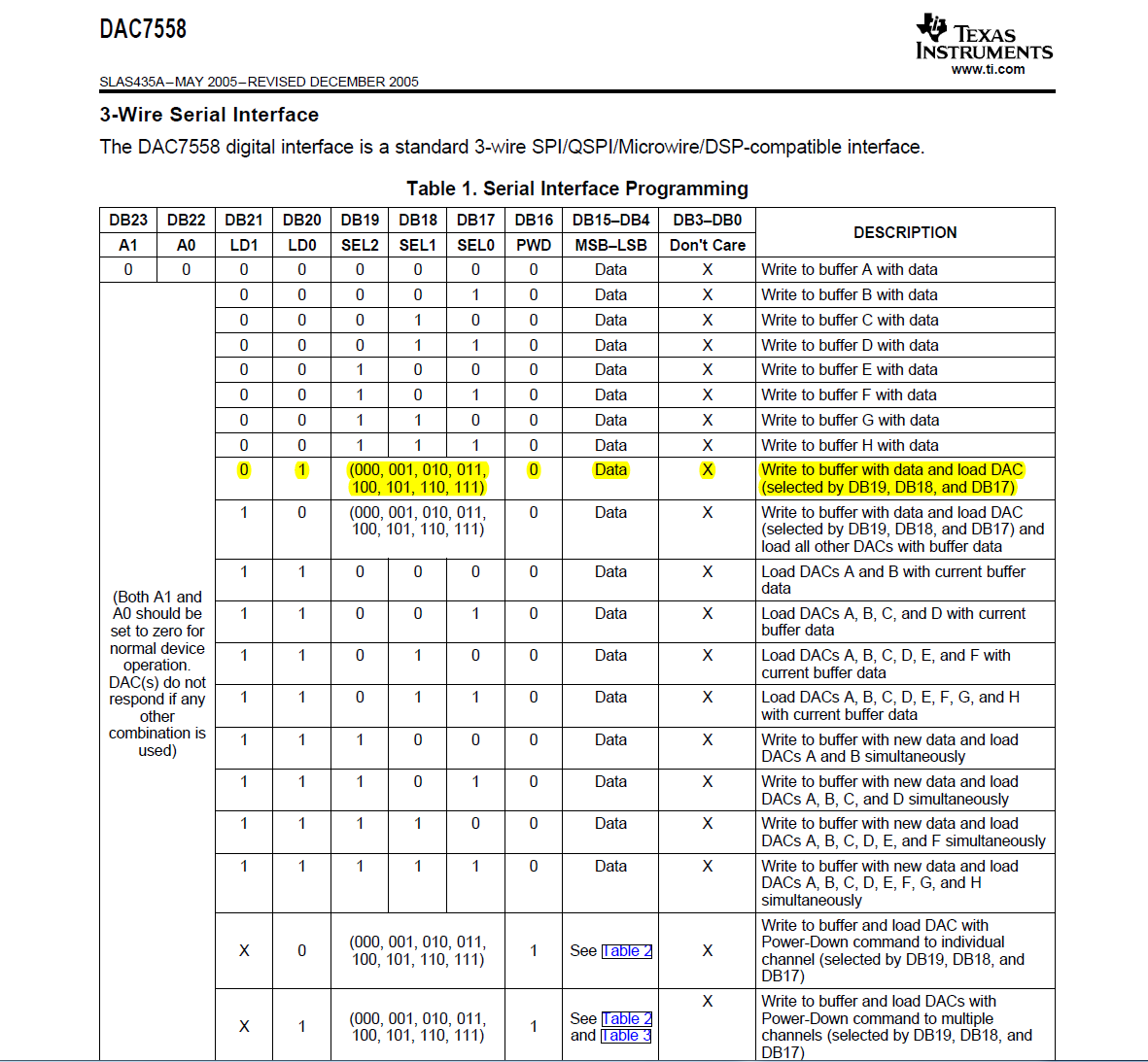
Problem: When firmware uses the SPI command "Write to buffer with data and load DAC (selected by DB19, DB18, and DB17)", the selected DAC channel will only change output voltage on odd writes (1st, 3rd, 5th, etc.).
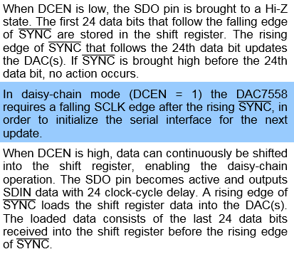
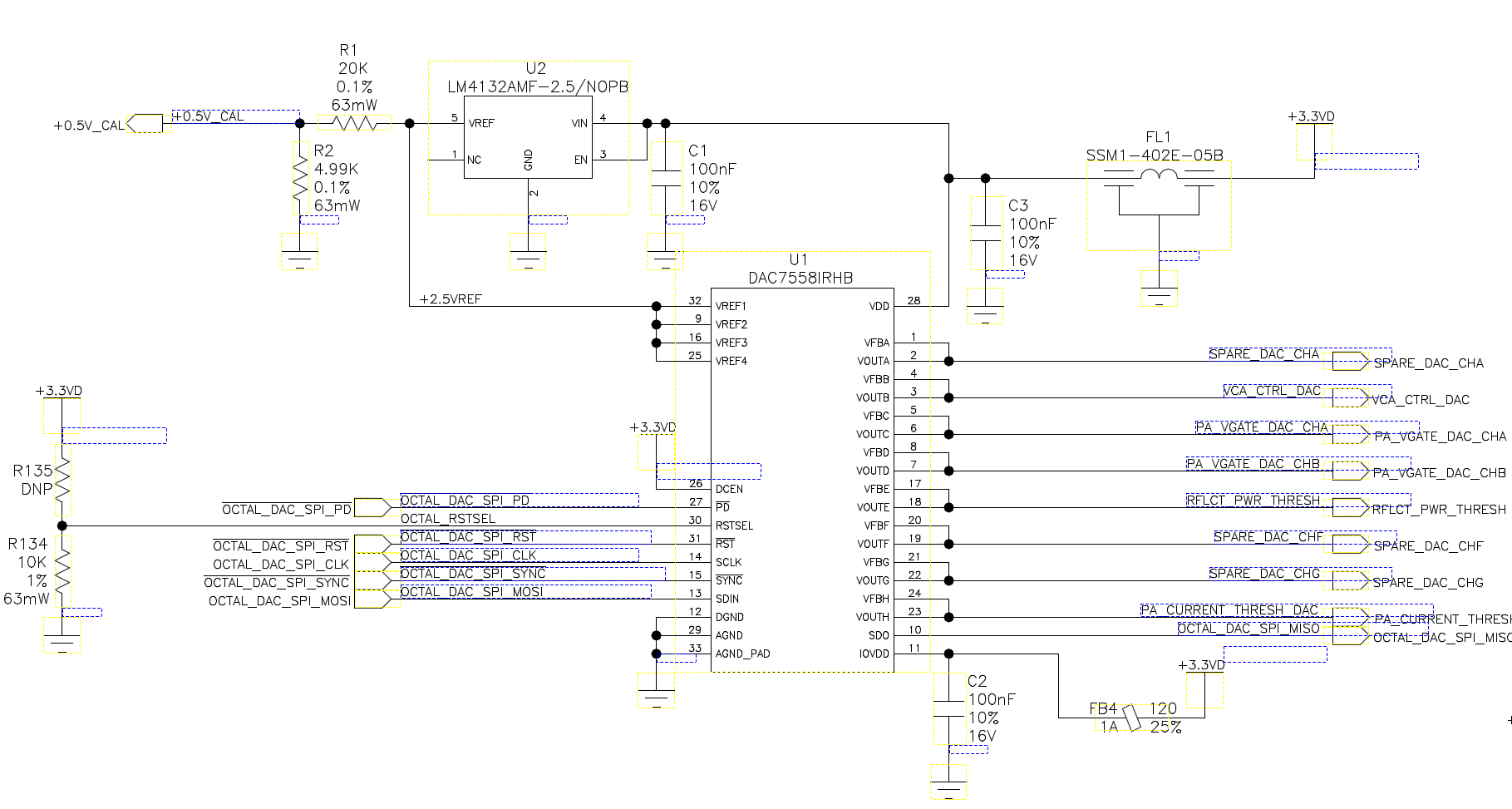
This is the first design I have used the DAC7558 (see schematic below for implementation). When the command does work for a selected channel, the output voltage is correct.
Tried changing the firmware to use separate SPI commands for “Write to buffer x with data”, then “Load DACs A, B, C, D, E, and F with current buffer data”. That combination resulted in no output on selected DAC channel.
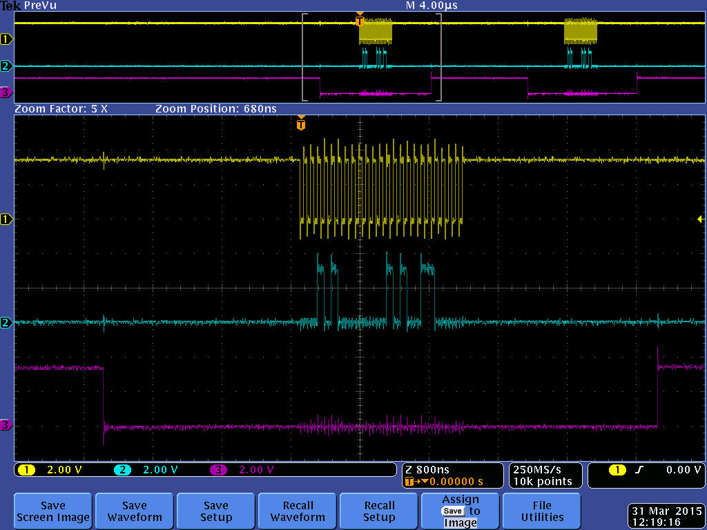
The timing of the physical SPI interface looks correct according to the datasheet parameters when analyzed with a logic analyzer.
Firmware is written in C and implemented in a soft core Microblaze processor running on a Xilinx Artix-7 FPGA. The SPI layer is implemented using a Xilinx SPI IP core.
While 2 writes of the SPI command does make the selected DAC channels output voltage change, what is the issue requiring that and for another design the separate commands of write to buffer and load DAC needs to work.
From dac_ifc.h:
/************************** Constant Definitions ****************************/

/*---- DAC Selection ------------------------------------------------------*/
#define DAC_SPARE_DAC_CHANNEL_A             0x00 // A
#define DAC_VCA_CONTROL_VOLTAGE             0x01 // B
#define DAC_PA_VGATE_CHANNEL_A              0x02 // C
#define DAC_PA_VGATE_CHANNEL_B              0x03 // D
#define DAC_REFLECTED_POWER_FAULT_THRESHOLD 0x04 // E
#define DAC_SPARE_DAC_CHANNEL_F             0x05 // F
#define DAC_SPARE_DAC_CHANNEL_G             0x06 // G
#define DAC_PA_CURRENT_THRESHOLD            0x07 // H
#define NUM_DAC_VALUES                      8

/*---- DAC Instruction -----------------------------------------------------*/
#define DAC_WRITE_BUFFER                    0x00 // Write data to buffer but DO NOT LOAD DAC
#define DAC_WRITE_BUFFER_LOAD_DAC           0x10 // Write data to buffer and then load selected DAC
#define DAC_WRITE_BUFFER_LOAD_ALL_DACS      0x20 // Write data to buffer and then load ALL DACS

#define DAC_SPI_CR_RESET_STATE              0x180 // Default value of SPI command register after reset

#define DAC_SPI_WAIT_DURATION               5000 // Maximum number of uBlaze cycles wasted waiting for SPI write to complete


From dac_ifc.c:
    // ----------------------------------------------------------------
    // Format 24-bit DAC Data
    switch (dacSelect) {
    case 0 : instruct = (uint32_t) DAC_WRITE_BUFFER_LOAD_DAC | (DAC_SPARE_DAC_CHANNEL_A << 1);
             break;
    case 1 : instruct = (uint32_t) DAC_WRITE_BUFFER_LOAD_DAC | (DAC_VCA_CONTROL_VOLTAGE << 1);
             break;
    case 2 : instruct = (uint32_t) DAC_WRITE_BUFFER_LOAD_DAC | (DAC_PA_VGATE_CHANNEL_A << 1);
             break;
    case 3 : instruct = (uint32_t) DAC_WRITE_BUFFER_LOAD_DAC | (DAC_PA_VGATE_CHANNEL_B << 1);
             break;
    case 4 : instruct = (uint32_t) DAC_WRITE_BUFFER_LOAD_DAC | (DAC_REFLECTED_POWER_FAULT_THRESHOLD << 1);
             break;
    case 5 : instruct = (uint32_t) DAC_WRITE_BUFFER_LOAD_DAC | (DAC_SPARE_DAC_CHANNEL_F << 1);
             break;
    case 6 : instruct = (uint32_t) DAC_WRITE_BUFFER_LOAD_DAC | (DAC_SPARE_DAC_CHANNEL_G << 1);
             break;
    case 7 : instruct = (uint32_t) DAC_WRITE_BUFFER_LOAD_DAC | (DAC_PA_CURRENT_THRESHOLD << 1);
             break;
    default: instruct = (uint32_t) DAC_WRITE_BUFFER_LOAD_DAC | (DAC_SPARE_DAC_CHANNEL_A << 1);
            break;
    }
    dacData <<= 4; // the four lsb's of the dac data are 'don't cares'
    dat_lo = (uint32_t)  dacData & 0x00FF;
    dat_hi = (uint32_t) (dacData & 0xFF00) >> 8;

    // Write Data (3-bytes) to SPI (DTR Register) - Write-only Register so don't read-back
    XSpi_WriteReg(spiPtr->BaseAddr, XSP_DTR_OFFSET, instruct); // msb of instruction shifted first
    XSpi_WriteReg(spiPtr->BaseAddr, XSP_DTR_OFFSET, dat_hi);
    XSpi_WriteReg(spiPtr->BaseAddr, XSP_DTR_OFFSET, dat_lo);   // lsb of low-byte data shifted last