This thread has been locked.

If you have a related question, please click the "Ask a related question" button in the top right corner. The newly created question will be automatically linked to this question.

ADC1256 stability

Other Parts Discussed in Thread: ADS1256

Hi,


We are using the ADS1256 to measure several NTC voltage and currents (voltage on Rsense).

The ADC is connected to a Zynq FPGA where we have an SPI module interfacing with the ARM core.


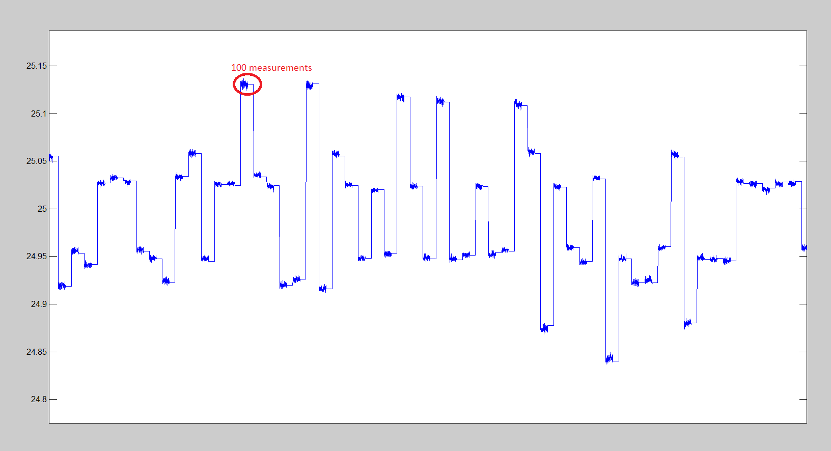
We observed a strange behavior when we restart the measurement: within in the loop the stability is quite good, around 0.01 C degrees , but in the next loop we randomly see an offset of 0.2C degree.


We did a measurement with a FIX resistor (we replaced the NTC) to check the stability. The temperature calculated from this resistor is around 25C. But we observed certain 'offset jumps' between measurement loops. See screenshot.


We were monitoring the SPI wires to see if it is a SW (FPGA / C-code) issue in data-postprocessing or these 'jumps' are already coming from the ADC.

Well, they are coming from the ADC.

Some measured hex values (measured on the AN01 input):

  1. Loop 1 .
  1. 0x6F 54 D1
  2. 0x6F 54 C2
  • Loop 2 .
  1. 0x6F D1 95
  2. 0x6F D2 0B
  • Loop 3.
  1. 0x6F 8F 2F
  2. 0x6F 8E 30


The differences within the loop is quite small, but between loops you see that the middle byte is changing.

We assume that the cause is somewhere around the configuration of the ADC that we use.

Here is the pseudo code of what we do:


Init() //run at every loop start

{

Cmd RESET

Wait_DRDY_HIGH

Cmd RESET

Wait_DRDY_HIGH

Cmd WREG DRATE, 0, 0xB0

Cmd STANDBY

Cmd WAKEUP

Wait_DRDY_HIGH

Cmd RREG DRATE

Cmd STANDBY

Cmd WREG GPIO, 0, 0

Wait_DRDY_HIGH

Cmd WREG ADCON, 0, 1

Cmd WREG STATUS, 0, 2

Wait_DRDY_HIGH

Cmd SELFCAL

}


//this runs in an FPGA VHDL FSM…

// same as the Fig19 in ADS1256 pdf (ver. Sept 2013)

Fpga_Meas()

{

Cmd WREG to change MUX

Cmd SYNC

Cmd WAKEUP

Cmd RDATA

Wait_t6;

RD data

}


Main()

{

Init()

For ( 10)

{

Cmd WAKEUP

For (100)

{

Fpga_Meas()

}

Cmd STANDBY

Wait_2sec

}


}


Note: this main function now mimics a more complex SW where we originally saw this issue.


Do you have any hints where to look for the cause?


Thanks,

   Andras


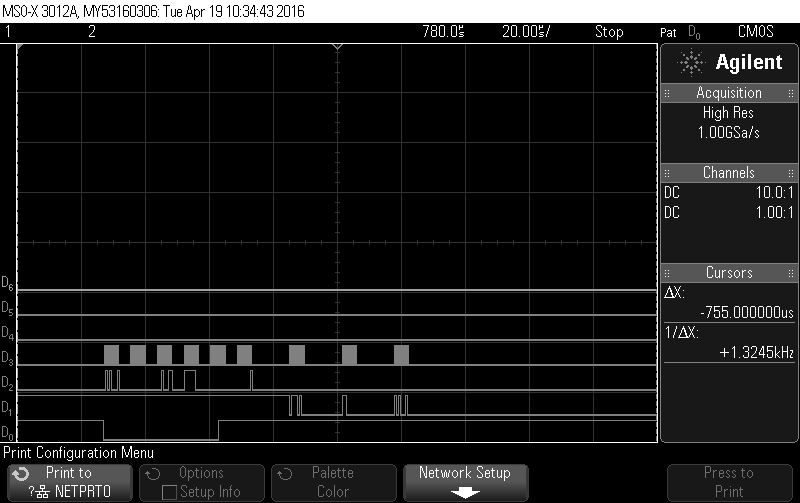
update: I have created some screenshots of the scope to show how the middle byte of the data is behaving.

D3: SCLK

D2: DIN

D1: DOUT

D0: DRDY

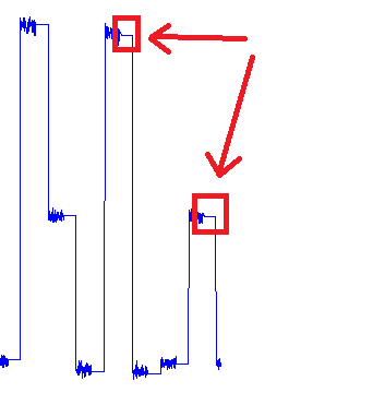
It also shows that the timing of DRDY-to-RDATA-retrival is always the same.

#1

#2

#3

#4

  • Hi Andras,

    It looks like the offset is changing with each code loop. Usually, resetting and restarting the device conversion would not affect the offset; however, in the case of the ADS1256, the offset can change because the ADS1256 performs self-calibration after a reset (even though ACAL = 0). Likely the OFC registers are being set to different values with each code loop. However, I don't know if self-calibration alone explains the 5-10 mV change in offset.

    Additionally, in your pseudo code, you have "Wait_DRDY_HIGH". Are you indeed waiting for /DRDY to go high?
    The device will be running self-calibration while /DRDY is high; therefore, I would recommending waiting until /DRDY goes low (indicating that self-calibration has completed). Also, performing reset once should be sufficient.

    Perhaps, after resetting the device, you could set the OFC registers to 0x00 to ensure that the offset is not changing as a result of self-calibration.

    Best Regards,
    Chris

  • Hi Chris,


    Thanks for the hints.

    At first we were also suspecting calibration to cause the different offsets in the loops. But there was no reset / restart between the loops, so in our understanding calibration SHOULD NOT have occured there.

    Based on your reply I have the feeling that somehow there is still some sort of calibration / adaption occuring at every loop.

    Can you confirm this?

    We noticed some noise on the using long cables for the AD input, obviously, but without cables we see the same scenario but with lower jumps.

    Anyhow we modified the loops as follows: removed WUP + Standby and added Offset reg write.


    Main()

    {

    Init()

    For ( 10)

    {

    Cmd WR reg OFC =0x00

    For (100)

    {

    Fpga_Meas()

    }

    Wait_2sec

    }

    }

    Without the long cable we saw this:

    Here you can still see some jumps, which are a bit greater than the 'noise band'. So the issue is it still there, just not so clearly visible.

    As for the 'Wait_DRDY_HIGH' in my pseudo code, I gave it a misleading name, it looks like this:

    while(read_dready() == DRDY_HIGH);

    So it exits at the falling edge of /DRDY. Which is what you also meant I think.

    Waiting for your feedback.

      Andras

  • Just to be clear: the init() function is only ran ONCE at the start. So calibration takes only place ONCE in our understanding.
    (in case my pseudo code was misleading)
  • Hi Andras,

    Your most recent pseudo-code should not trigger a re-calibration.

    Calibration should only occur in these circumstances:

    • After power-up
    • After a RESET (SPI "RESET" command byte, SCLK reset pattern,or RESET pin toggle)
    • After writing to a register that changes the data rate, PGA gain, or buffer status while ACAL is enabled.
    • Or after issuing one of the SPI calibration commands.

    Here are some other things you can check...

    Are you enabling the input buffer (by setting BUFEN high in the STATUS register)?
    Your earlier pseudo-code indicated that BUFEN was set to 1. It might be worthwhile to read back the STATUS register and ensure this is set correctly. If the buffer is not enabled, the ADC's input impedance will be lower and input bias current may be higher.

    If you collect 1000 continuous samples, do you see any measurement drift (or jumps in offset) or are the results good?
    From the current 100 samples in your loop the continuous samples appear stable. It makes me wonder if there is some event between loops that occurs (maybe something is causing a spike in power supply current).

    Is there any other operation occurring between code loops?
    For example, do you stop and restart conversions, or power down the ADC or some other component in the system?

    Have you monitored the power supply and reference voltages to make sure they are stable between loops?

    What are you using to excite the NTC/resistor? Is it stable?

    Do you have a filter on the ADC input, is it high impedance?
    It's interesting that the cable length is affecting the offset....This would make me question if there is a bias or leakage current interacting with an impedance in the input signal path.


    Another thing I noticed is that your plot showed flat regions in the temperature result. Is this just a "placeholder" (to indicate that time has passed between conversions) or is this real ADC data (which looks so perfect that I would question the validity of this data)?

    I'm sorry for the list of questions, but at the moment I'm still trying to get a sense of your circuit configuration and what you've already done in terms of troubleshooting.

    Best Regards,
    Chris

  • Hi Chris,


    Thanks for the hints.

    BUFEN was enabled, we checked this earlier. The flat regions on the plots are because we had a sleep() between the loop iterations, so these flat sections are just coming from the plot.

    We use a reference voltage source for the NTC, and we had already these jumps on this line. We fixed that and now the jumps are gone.

    Thanks again.

      Andras