This thread has been locked.

If you have a related question, please click the "Ask a related question" button in the top right corner. The newly created question will be automatically linked to this question.

ADS1262: Unable to capturing serial data coming DOUT/DRDY pin

Other Parts Discussed in Thread: ADS1262

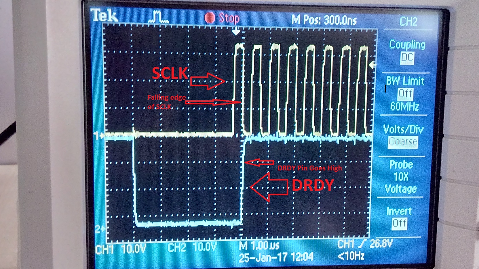
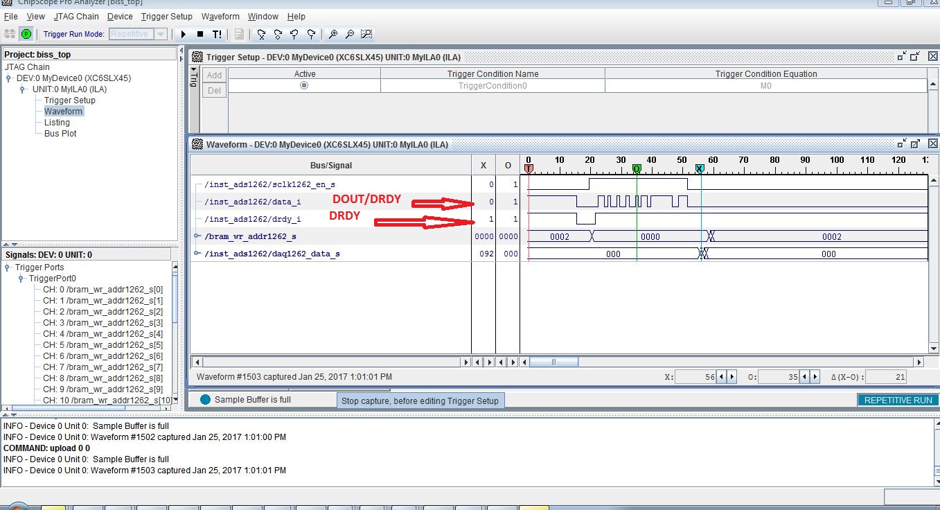
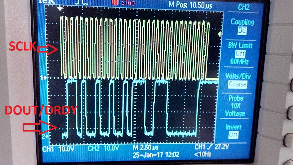
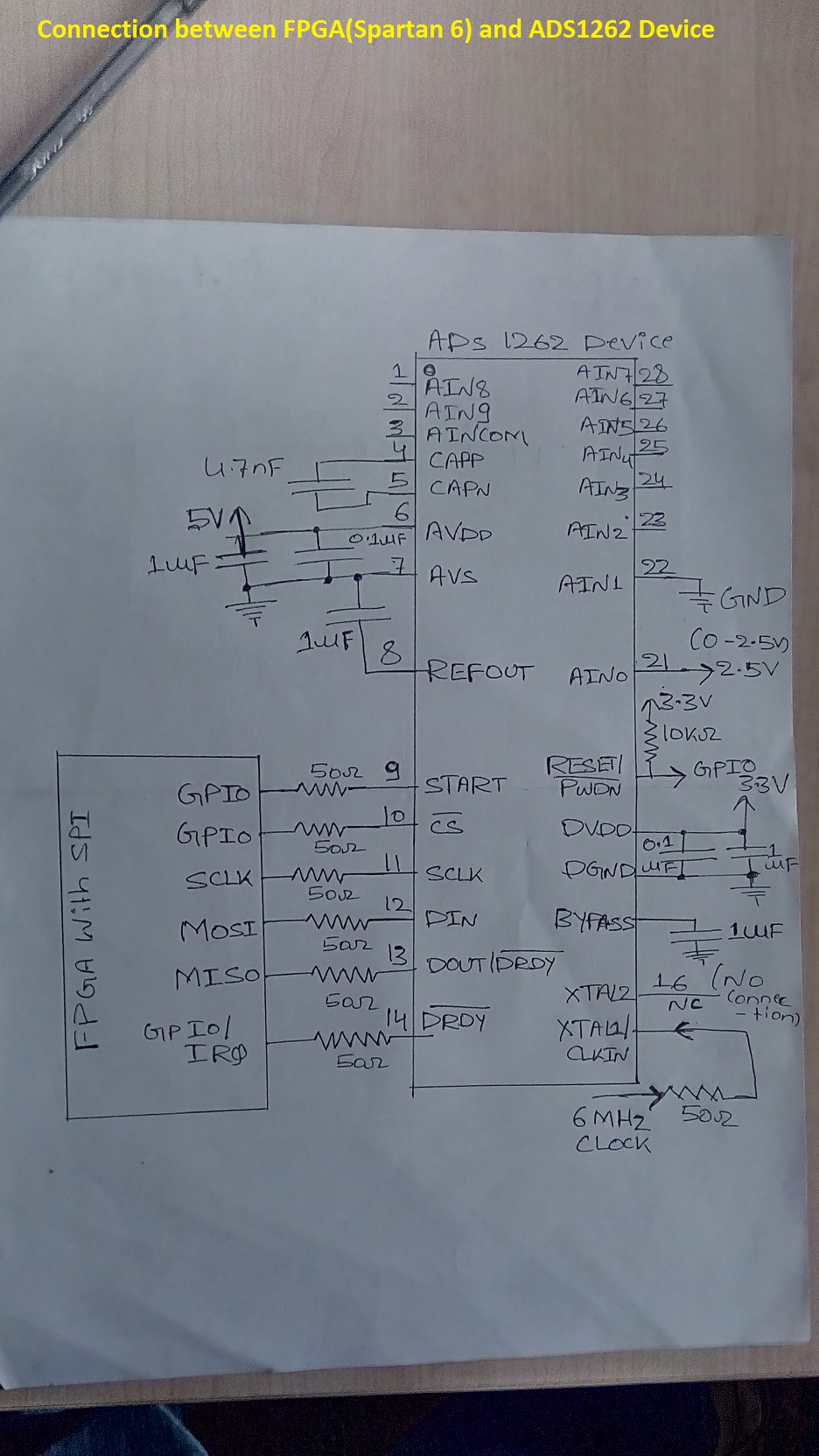
I have been using ads 1262 connecting with FPGA .I have written code in VHDL, data conversation can be seen by checking pin DOUT/DRDY, but unable to capturing serial data coming DOUT/DRDY pin.I have configured all analog and digital  voltages as per data sheet. I am using shift register method to update data(SIPO Register).

The below will code i written in VHDL

when start_adc_conv_st =>
if(start_i = '1') then
start <= high;
start_adc_counter <= start_adc_counter + 1;
if(start_adc_counter = 4) then
start <= low;
adc_1262 <= start_adc_conv_st1;
end if;
else
start <= low;
adc_1262 <= start_adc_conv_st;
end if;
when start_adc_conv_st1 =>
if(start_adc_counter = 8 ) then
start <= high;
start_adc_counter <= 0;
adc_1262 <= drdy_detect1_st;
else
start_adc_counter <= start_adc_counter + 1;
start <= low;
adc_1262 <= start_adc_conv_st1;
end if;
when drdy_detect1_st =>
if(drdy_i = '1') then
adc_1262 <= drdy_detect2_st;
else
adc_1262 <= drdy_detect1_st;
end if;

when drdy_detect2_st =>
if(drdy_i = '0') then
sclk_enable_s <= high;
bram_wr_cntr <= 06;
-- drdy_wait_cntr <= 0;
-- test_data <= (others => '0');
bram_wr_addr_s <= (others => '0');
adc_1262 <= data_collect_st;
else
adc_1262 <= drdy_detect2_st;
end if;
when data_collect_st =>
if(ch1_cntr = low_cnt) then
sclk_enable_s <= low;
bram_wr_en_s <= high;
adc_1262 <= bram_write_data_st;
else
if(rd_en1_i = '1') then
received_data <= received_data(30 downto 0) & data_i;
ch1_cntr <= ch1_cntr - 1;
if(ch1_cntr = 5) then
sclk_enable_s <= low;
end if;
end if;
adc_1262 <= data_collect_st;
end if;


when bram_write_data_st =>
if(bram_wr_cntr = low_cnt) then
bram_wr_en_s <= low;
ch1_cntr <= 32;
cntr <= 0;
received_data <= (others => '0');
adc_1262 <= drdy_detect1_st;
else
bram_wr_addr_s <= bram_wr_addr_s + 1;
bram_wr_cntr <= bram_wr_cntr - 1;
adc_1262 <= bram_write_data_st;
end if;
when others =>
null;
end case;
end if;
end process;

Thank you inadvance

  • Hi Shambhu,

    Welcome to the TI E2E Forums!

    Would it be possible for you to share some oscilloscope or logic analyzer screenshots of the SPI communication?
    You'll have to pardon me, but I'm not very familiar with VDHL....Besides, often times I'll find it more useful to look at the actual communication, as the code doesn't always show the problem.

    Are you seeing ANY response from the ADS1262 on the DOUT pin?

    Also, would it be possible to see a schematic of your circuit?


    Thanks and Best Regards,
    Chris

  • Hello Christopher Hall 

    Thank you for your replay.

    I have been using ADS 1262 connecting with FPGA .My End-application will be acquiring data from Load Cell.I have configured all analog and digital  voltages as per data sheet. I am using ADS 1262 in default configuration mode.The one more problem I am facing is that  For writing  data to the register for programming, DRDY pin  is always HIGH.As per the data sheet we have read DRDY PIN High to Low transition,the shifting input serailly through DIN PIN,after first clock DRDY Pin is always High(Using Parallel in Serial Out ). I am reading  data from   DOUT/DRDY is in Serial  in Parallel Out fashion.

    As per default configuration mode following will be the specification

    1. ADS 1262 is using continuous  conversion mode.

    2.All register used in default configuration settings.

    3.I am using single ended connection.

    4. AIN 0 pin I am applying ( 0-2.5 V) DC Voltage,using the potentiometer (Variable resistor) vary input voltage range(0- 2.5 V) and AIN 1 is grounded.

    5.Register settings -Default Settings

    6. input signal- ( 0-2.5 V) DC Voltage(PIN no 21 ---AIN 0)

    7.Supply voltages - (AVDD - 5V), ( AVSS - GND),(DVDD-3.3V),(DGND - GND)

    8.DIN and CS Pins of ADS 1262 tied LOW through  GPIO PINS of FPGA.

    9.START and RESET/PWDN is tied HIGH through  GPIO PINS of FPGA.

    10.XTAL 1/CLKIN1 is connected to 6 MHz clock through 50 ohm resistor.

    11..XTAL 2 is OPEN(Float Connection)


    These shown in Connection diagram between FPGA and ADS 1262 image attached.

  • Hi Shambhu,

    Thanks for sharing the additional information and screenshots!

    From my perspective it would appear like the ADS1262 is responding correctly. Therefore, is the issue your having that the FPGA is not reading the same data as seen on the oscilloscope or that the data is not making sense? I'm sorry, I'm not quite sure I understand the problem.


    One thing I noticed, you appear to only send 32 SCLKs when reading the data. However, with the default register settings you will need to send a total of 48 SCLKs to clock out the STATUS, DATA, and CRC bytes (as shown below). At the moment you may only be getting the STATUS, DATA1, DATA2, and DATA3 bytes....

    Another thing to check would be the SPI mode your using. The ADS1262 uses SPI mode 1 (CPOL=0, CPHA=1); therefore, make sure you are reading the data on falling edge of SCLK.

    The /DRDY behavior also looks correct...It typically goes low when a conversion is completed and then returns after after the first SCLK. So I don't see any issues there.

    Aside: From the oscilloscope screenshot the first byte back from the ADS1262 is the STATUS byte, and it appears to have the value of 0x69. This would indicate that the conversion data is new, that you're using an external clock, and that the input voltage is violating the PGA's common-mode voltage (low-side). This makes sense, because you've connected the negative input to ground. To ensure linear PGA operation, you will need to apply a higher voltage to AIN1 or bypass the PGA.


    Best Regards,
    Chris

  • Hi Christopher Hall

    Thank you for your reply.

    The data  reading problem is solved.The one more problem I am facing is that  for writing  data to the register for programming, DRDY pin  is always HIGH.As per the data sheet we have read DRDY PIN High to Low transition,then shifting  serailly input through DIN PIN,after first clock DRDY Pin is always High(Using Parallel in Serial Out ),because I want to increase sampling rate of ADS 1262 IC I have programmed like below

    1.Selection of Data  rate,PGA enable and GAIN[2:0]

    For this use Mode2 Register (address = 05h)

    OPCODE 1 = 45h, OPCODE 2 =00h,REG DATA1= 5Dh,REG DATA2=00h,I have selected following

    Bit 7 is '0'  for PGA enable

    Bit6:4  is '101'  for GAIN[2:0] -----32V/V

    Bit3:0  is '1101'  for Data Rate ---14400 SPS

    Bit 7 Bit6:4 Bit3:0 = '01011101'= 5Dh

    Thanks in advance for  your reply.

    Regards ,

    Shambhu Hosamani

  • Hi Shambhu,

    shambhu hosamani said:
    OPCODE 1 = 45h, OPCODE 2 =00h,REG DATA1= 5Dh,REG DATA2=00h,I have selected following

    In this case, you're only writing to a single register; therefore, you do not need to clock in the "REG DATA2" byte. You only need to provide a single data byte here!

    After you send the above WREG command, have you tried using the RREG to read back the register configuration for verification?

    Best Regards,
    Chris