This thread has been locked.

If you have a related question, please click the "Ask a related question" button in the top right corner. The newly created question will be automatically linked to this question.

ADS1298: ADS1298 - Test Signal Amplitude varies with number of enabled channels

Part Number: ADS1298
Other Parts Discussed in Thread: REF5025

Hi

I am using the ADS1298 and I am struggling to get a consistent test signal amplitude. The Test signal amplitude varies depending on the number of channels enabled. Is this correct?

My set up is as follows:

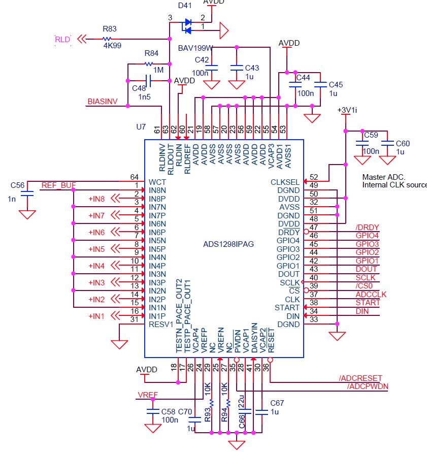
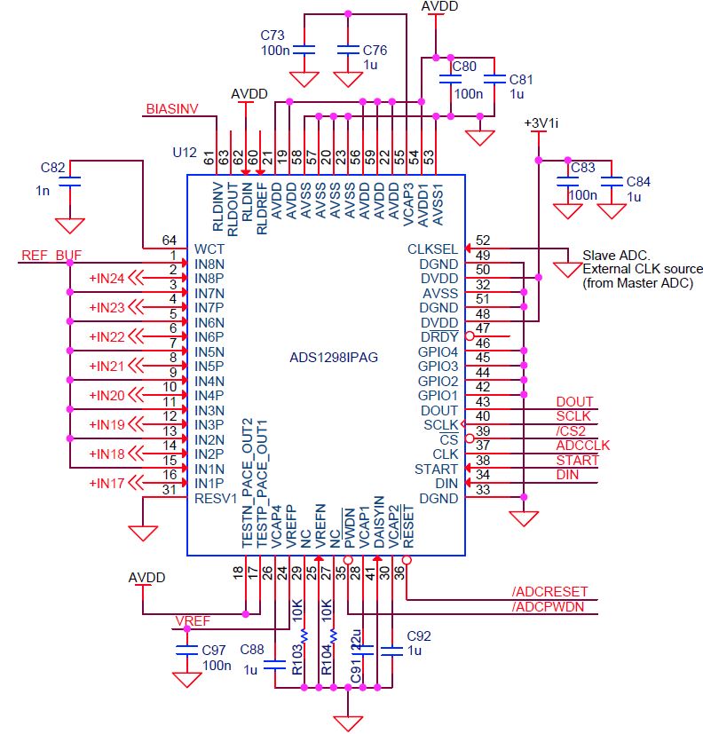
- I have 4 ADS1298 operating in multiple read back mode. The first ADS1298 supplies the clock signal to the other 3.

- Reference voltage is external, 2.5V  (REF5025, using suggested circuit in data sheet)

- AVDD and DVDD: Supply voltage 3.1V.

The gain has been set to 6 (default), so I am expecting a Test voltage amplitude of +-1.04mV. (2.5/2400 V).  I am able to measure this on the first ADC only when one channel is enabled. If all 8 channels are enabled, I measure 1.4mVp-p. This behaviour varies across all four ADS1298. On the second ADS1298, I measure the expected voltage when all 8 channels are enabled.

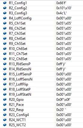
The registers (for the first ADC) are as follows (ADC 2-4s have Config 1 = 0x46, Config 3 = 0x40) :

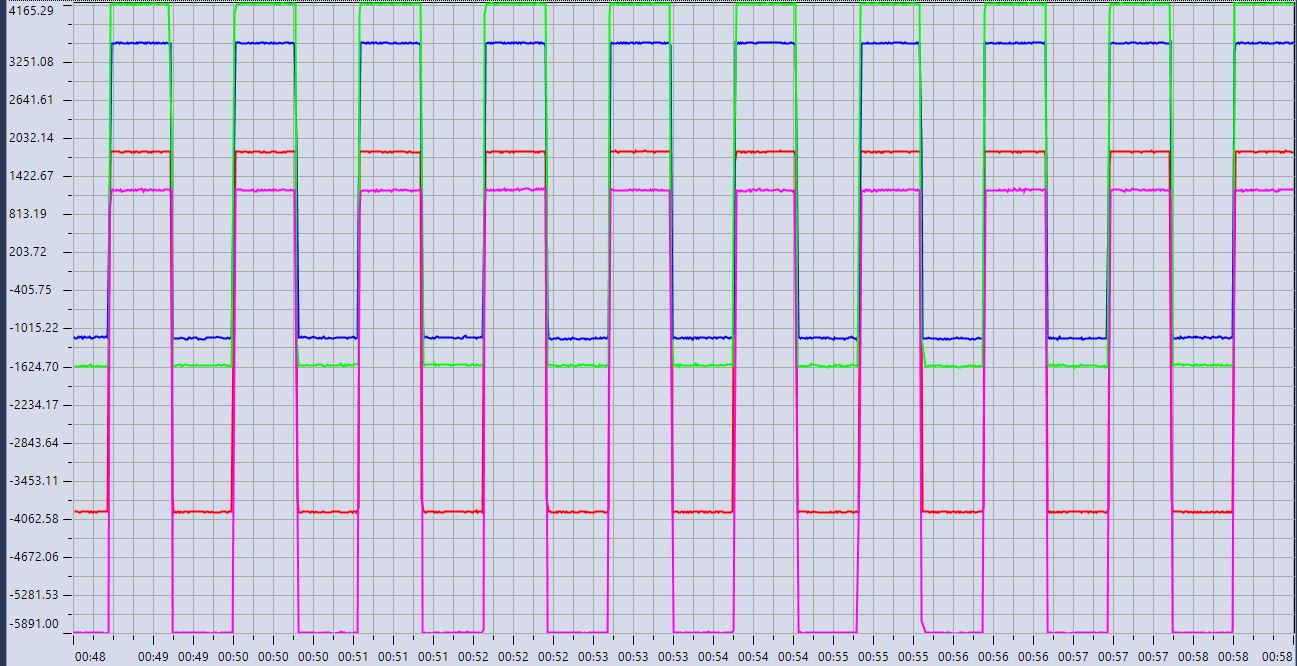
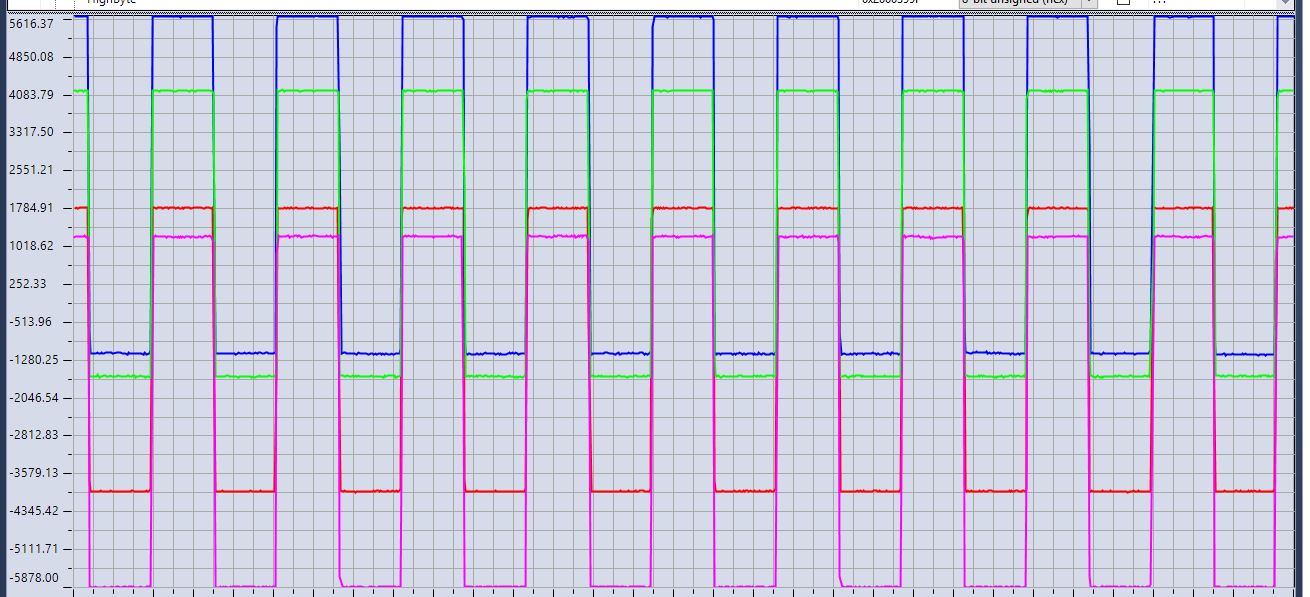
The Raw ADC data for Channels 1 (blue trace), 9 (pink), 17 (green) and 25 (red) (I.E. Ch 1 of each ADS1298 chip) is shown below. Ignoring the offset, you will notice each channel has a different peak-peak amplitude.


The graph below shows the ADC data when only Channel 1 of ADC 1 is enabled and the remaining 7 channels are powered down (Bit 7 of CHnSET set). The remaining 3 ADCS still have all channels enabled.

You will notice that the blue trace (Channel 1) now has a  maximum ADC value of ~ 5616, instead of ~3700 as shown in the previous graph. The only difference in the set up is Channels 2-8 are powered down.


Can anyone offer any insight into this issue?

Thank you for your help.

kind regards,

Geoff

  • Hello Geoff,

    Can you please share your schematic?

    Brian
  • Hi Brian

    Thanks for your reply. Here are the schematics for 2 of the ADS1298 chips (ADC 1 (Master) & 2 (Slave)). The other two ADS1298 chips are connected as per ADC 2. The Vref  circuit is the same as the Data sheet, Figure 32 (REF5025 plus buffer).

    I have done some more testing and when all the channels are set to the Test signal input, each channel records different amplitudes. I have tested using the internal reference and an external reference and the behaviour is the same  - each channel recording a different value for the test signal. 

    In normal operation, when I apply a known test signal to the ADC inputs, the ADC data is correct. I have also read back all the registers to confirm that they are being set to the correct values, which they are.

    Thanks for your help.

    Regards,

    Geoff

  • Hello Geoff,

    This is a known issue relating to the connections of the TEST_PACE_OUT1 and TEST_PACE_OUT2 pins. Although the datasheet currently says to tie those inputs to AVDD if unused, we ask that you actually leave those pins floating to measure the internal test signal correctly. We are working to get the datasheet updated. This issue will not affect your ability to measure normal signals through the channel inputs.

    Looking at your schematic it looks like those pins are hard tied to AVDD so you will probably not be able to remove them easily on this board to validate my claim, but if you do another board revision, please leave the pins floating. I apologize for the inconvenience this has caused.

    Regards,
    Brian Pisani
  • Hello Brian

    Thank you. With some very, very careful soldering, I lifted the two TEST_PACE_OUT pins on each chip. The test signals are now all the same amplitude and are behaving as expected.

    Thanks again. I appreciate your help.

    Kind regards,
    Geoff
  • Hi,
    we're facing a similar problem as described above.
    We're using the internal test-signal of the ADS to do a quick production-test after manufacturing of the board. But we see a differing offset for each channel for each device when we measure the testsignal. In our application we've left the TEST_PACE_OUT1 and TEST_PACE_OUT2 floating, so that should be correct. The amplitude of the measured testsignal is correct, but we're wondering whether or not the differing offset for each channel is an issue (e.g. something is wrong with the design or the board) or that we can safely ignore this and only test on the amplitude of the signal.
    I hope someone can help in this, regards,
    Herman
  • Herman,

    This is normal behavior for the device. The offset error between the channels may vary, but should remain either within or relatively close to the datasheet specification for input referred offset error.

    Brian