Other Parts Discussed in Thread: ADS7953, , ADCPRO
Tool/software: Linux
Dear TI E2E Community,
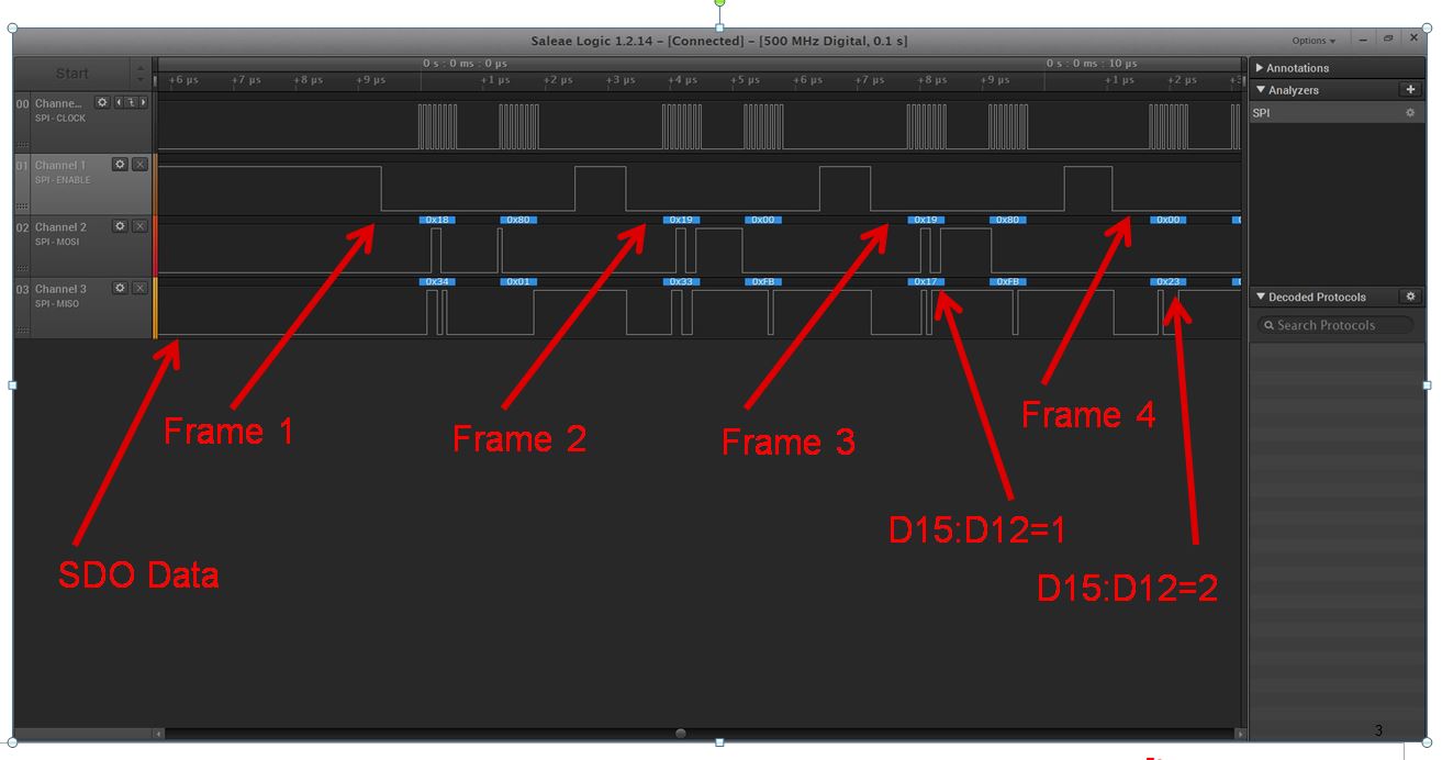
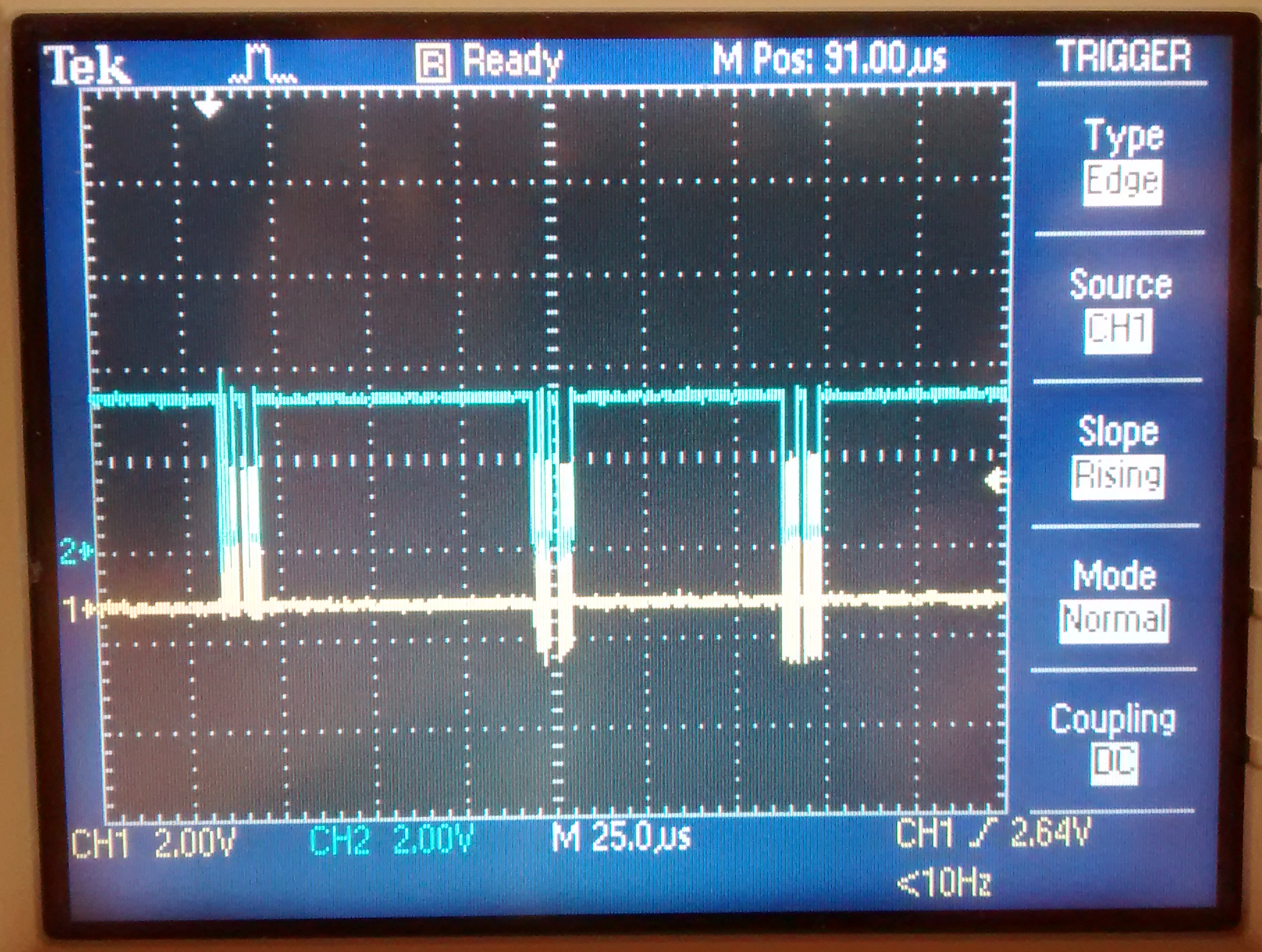
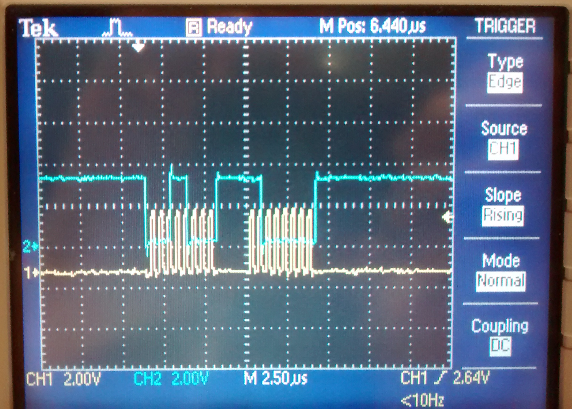
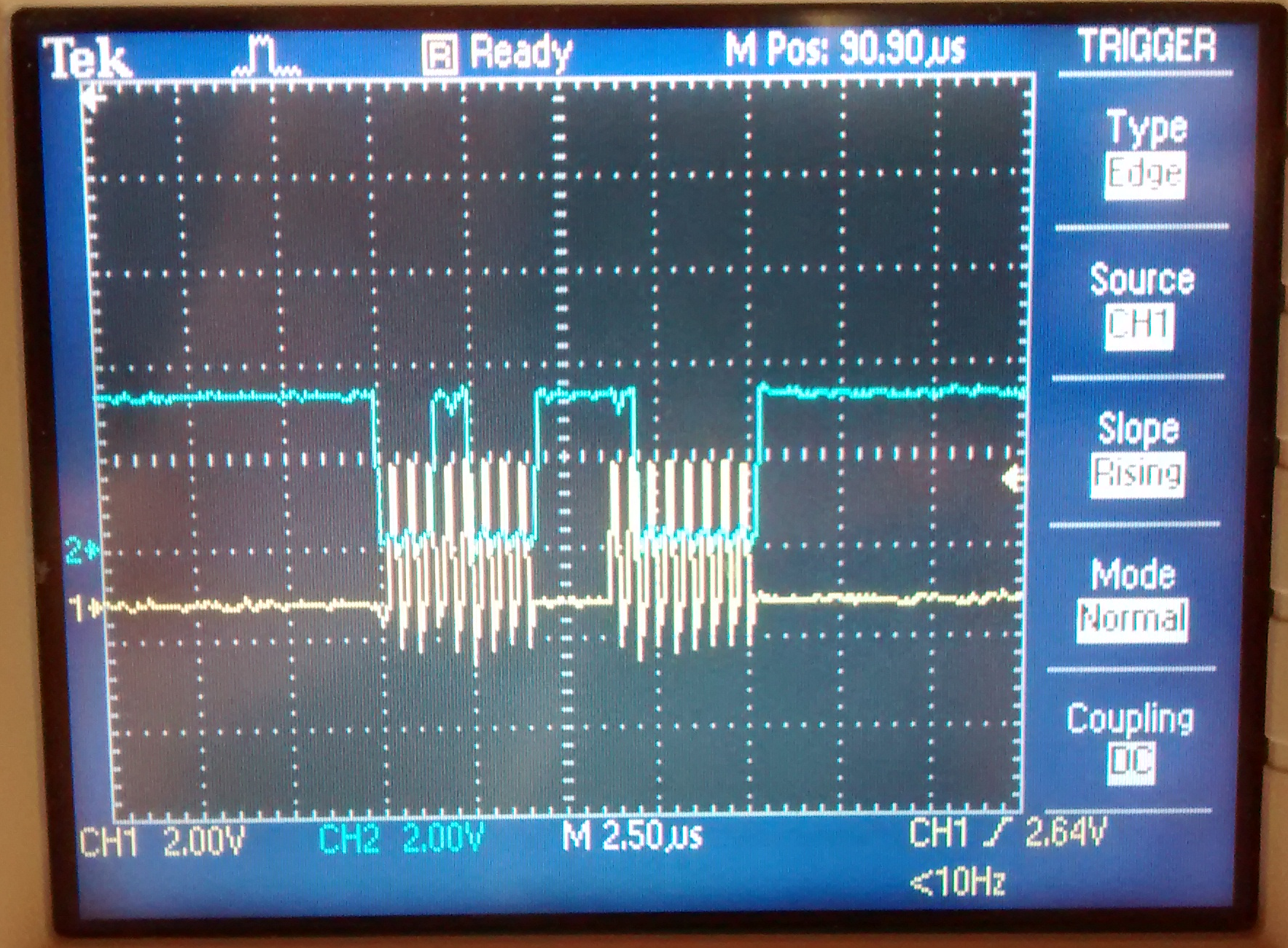
I'm trying to get data out of my ADS7953 with no success. My setup is composed by:
- an i.MX6 EVB connected via SPI to the ADS7953 evaluation board (ADS7953EVM-PDK)
- a Freescale Linux image based on the following Kernel: 4.1.43-fslc+ga73554d
The driver of the ADS (ti-ads7950.c) is properly installed, I see the following hierarchy:
root@imx6qdlsabresd:~# ls -la /sys/bus/iio/devices/iio\:device0/
drwxr-xr-x    6 root     root             0 Jan  1  1970 .
drwxr-xr-x    4 root     root             0 Jan  1  1970 ..
drwxr-xr-x    2 root     root             0 Sep 29 09:30 buffer
-r--r--r--    1 root     root          4096 Sep 29 09:30 dev
-rw-r--r--    1 root     root          4096 Sep 29 09:30 in_voltage0_raw
-rw-r--r--    1 root     root          4096 Sep 29 09:30 in_voltage10_raw
-rw-r--r--    1 root     root          4096 Sep 29 09:30 in_voltage11_raw
-rw-r--r--    1 root     root          4096 Sep 29 09:30 in_voltage12_raw
-rw-r--r--    1 root     root          4096 Sep 29 09:30 in_voltage13_raw
-rw-r--r--    1 root     root          4096 Sep 29 09:30 in_voltage14_raw
-rw-r--r--    1 root     root          4096 Sep 29 09:30 in_voltage15_raw
-rw-r--r--    1 root     root          4096 Sep 29 09:30 in_voltage1_raw
-rw-r--r--    1 root     root          4096 Sep 29 09:30 in_voltage2_raw
-rw-r--r--    1 root     root          4096 Sep 29 09:30 in_voltage3_raw
-rw-r--r--    1 root     root          4096 Sep 29 09:30 in_voltage4_raw
-rw-r--r--    1 root     root          4096 Sep 29 09:30 in_voltage5_raw
-rw-r--r--    1 root     root          4096 Sep 29 09:30 in_voltage6_raw
-rw-r--r--    1 root     root          4096 Sep 29 09:30 in_voltage7_raw
-rw-r--r--    1 root     root          4096 Sep 29 09:30 in_voltage8_raw
-rw-r--r--    1 root     root          4096 Sep 29 09:30 in_voltage9_raw
-rw-r--r--    1 root     root          4096 Sep 29 09:30 in_voltage_scale
-r--r--r--    1 root     root          4096 Sep 29 09:30 name
lrwxrwxrwx    1 root     root             0 Sep 29 09:30 of_node -> ../../../../../../../../../../firmware/devicetree/base/soc/aips-bus@02000000/spba-bus@02000000/ecspi@02008000/adc@0
drwxr-xr-x    2 root     root             0 Sep 29 09:30 power
drwxr-xr-x    2 root     root             0 Sep 29 09:30 scan_elements
lrwxrwxrwx    1 root     root             0 Sep 29 09:30 subsystem -> ../../../../../../../../../../bus/iio
drwxr-xr-x    2 root     root             0 Sep 29 09:30 trigger
-rw-r--r--    1 root     root          4096 Jan  1  1970 uevent
I tried to follow the instructions here with no success: http://processors.wiki.ti.com/index.php/Linux_Core_ADC_Users_Guide
When I try to execute a cat on channel #0 I got 0 as result, when I try to execute a cat on any other of the 11 channels I got:
root@imx6qdlsabresd:~# cat /sys/bus/iio/devices/iio\:device0/in_voltage7_raw
cat: read error: Input/output error
I have configured the Kernel device tree as following:
&ecspi1 {
	fsl,spi-num-chipselects = <1>;
	cs-gpios = <&gpio4 9 0>;
	pinctrl-names = "default";
	pinctrl-0 = <&pinctrl_ecspi1>;
	status = "okay";

        adc@0 {
 	compatible = "ti,ads7953";
 	reg = <0>;
 	#io-channel-cells = <1>;
 	vref-supply = <3000>;
 	spi-max-frequency = <20000000>;
        };
};
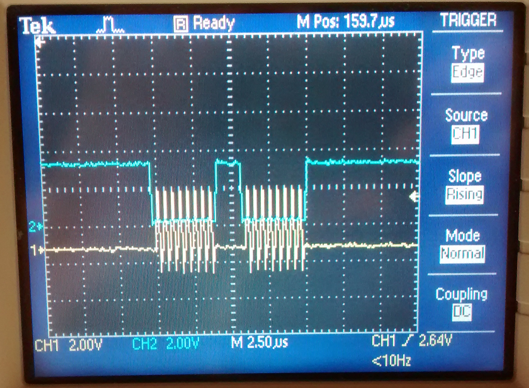
Is it ok to specify a vref of 3V? Is it ok to use an SPI frequency of 20MHz?
Thanks in advance for your help
EDIT: the vref is expressed in mV, since it's provided by the ADS7953EVM-PDK I'm not sure if the vref-supply field can be useful or not
Regards,
Fabio Emiliani