This thread has been locked.

If you have a related question, please click the "Ask a related question" button in the top right corner. The newly created question will be automatically linked to this question.

ADS1258: ADS1258 REFERENCE VOLTAGE RELATED QUESTION

Part Number: ADS1258
Other Parts Discussed in Thread: REF5025, REF5050

Hi,

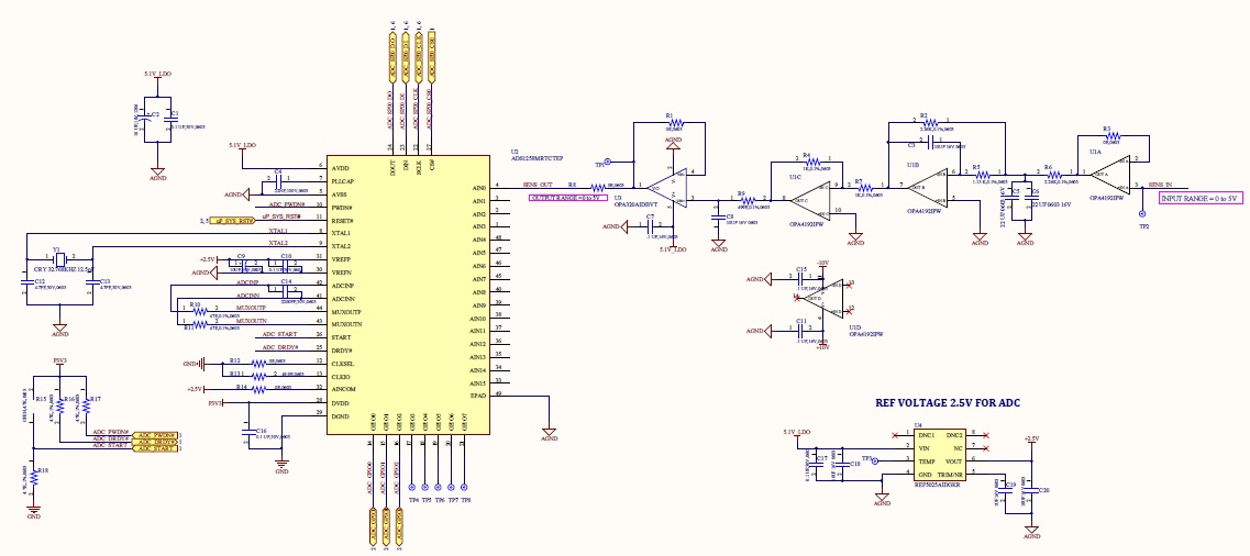
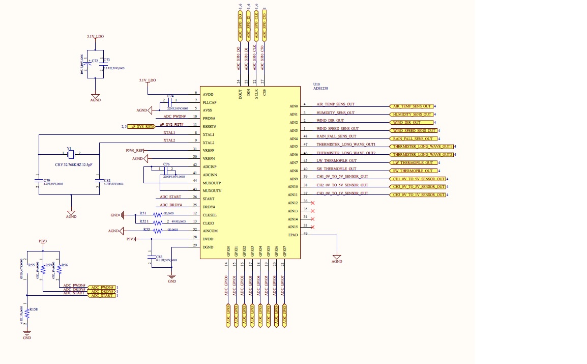
     We are using ADC (ADS1258) for one of our project.we have following doubts

1) Our ADC signal input is single ended and voltage level is 0-5V. We are giving VREFP is 5V through LDO (REF5050AIDGKR). Is it correct or need te give +2.5V and -2.5V as a ref voltage

for your reference we are attaching our schematics.

2)External Chopping is require or what we connected is correct?

3) My ADC input signal is uni polar (0-5V) and i given VREFP is +5V and VREFN is GND. I would like to utilise full bandwidth of ADC Scale in straight binary format (000000h to FFFFFFh). How to use this configuration.

Please verify this schematics and  Can you  give me clarification

  • Hi Renga,

    I'd be glad to help clarify.

    1. Your reference voltage is correct. VREFP and VREFN need to be within range of AVDD and AVSS, so you would only use a bipolar reference voltage when using bipolar supplies.

    2. I'm not sure what you mean by "external chopping". The ADS1258 can internally chop the input signal to help remove offset voltages, no external circuitry is required.

      The only recommendation I would have for your input circuit is to consider adding buffers between the MUXOUT and ADCIN pins. The ADC modulator inputs are not high-impedance, so any inputs that are not coming from low-impedance sources could have increased gain error when unbuffered.

    3. The ADS1258 expects differential inputs and will provide a two's compliment binary output that ranges from 800000h to FFFFFFh when the input is between -1.06*VREF and 0V, and 000000h to 7FFFFFh when the input is between 0V and +1.06*VREF.

      The only way to you would be able to utilize most of the ADC output codes for a 0-5V input signal would be to...

      1. Use a 2.5V reference (such has the REF5025 - which I believe is pin for pin compatible with the REF5050)

        and

      2. Connect the "negative" input (AINCOM, for example) to 2.5V. In this way, when the input is 0V the ADC will measure -2.5V deferentially and provide an output code near -FS, and when the input is 5V the ADC will measure 2.5V differentially and provide an output code near +FS.


    I hope that helps!

    Best regards,
    Chris

  • Analog inputs (12 channels Single Ended) driven through Buffer amp.


    Do I still need one more buffer amp stage between MUXOUT and ADCIN as your recommendation? Schematic attached.

    ADC input range is 0-5V, as per your recommendation tied VREFP pin to +2.5V , VREFN pin to AGND and AINCOM to +2.5V. Expecting Full scale range (000000 to FFFFFF). Hope I am correct.

  • Hi Renga,

    It is not a problem to provide your external signal conditioning circuitry prior to connecting to the AIN0 pin.
    Just keep in mind that if you use any of the other input pins that they too might need to be buffered. The advantage of buffering between the MUXOUT and ADCIN pins is that you can have a single buffer circuit that potentially works for all 16 analog inputs, instead of having to place 16 buffers; one on EACH input.

    ADC Output Codes
    Even for single-end inputs signals, the ADS1258 will deferentially compare your input (AIN0) to AINCOM and provide you will the measurement result. For a 0V input the ADC will measure -2.5V and the output code will be around 0x880000...Keep in mind that the output code is two's-compliment binary and that the most negative code (0x800000) will be reserved for -1.06*VREF or -2.66V since the ADS1258 can measure signals slightly larger than VREF.

    For a 2.5V input, the ADC will deferentially see a ~0V signal and the output code will be near 0xFFFFFF (-1) or 0x000000 (0).

    When your input signal is 5V, the ADC will deferentially see a 2.5V signal and the output code will be near  0x780000. The most positive code (0x7FFFFF) will be reserved for +1.06*VREF or +2.66V since the ADS1258 can measure signals slightly larger than VREF.

    Where in your circuit do AGND (AVSS) and GND (DGND) connect?
    I would recommend connecting these pins together CLOSE to the ADC! If you have any significant impedance (inductance) between this pins it can cause noise performance to degrade. And, if AGND and DGND develop any significant voltage difference it may also prevent the ADS1258 from working properly, or in some cases even damage the device.

    ...When possible, I try to use a single GND plane for both analog and digital circuits. To avoid cross-talk between these domains, I will partition the circuitry on my PCB so that analog and digital circuits occupy different regions on my board. This is usually sufficient to keep digital return current noise out of the analog circuit and it usually improves EMI performance as well.


    Best regards,
    Chris

  • Thanks for your valuable feedback.