This thread has been locked.

If you have a related question, please click the "Ask a related question" button in the top right corner. The newly created question will be automatically linked to this question.

TLC0820A: Simplest ADC control possible.

Part Number: TLC0820A
Other Parts Discussed in Thread: SN74HCT373

Hi-

I am looking at using a TLC0820 ADC.

I am trying to minimize external the components needed to control the ADC conversion.

I have 2 requirements:

Use 1 control signal (The control signal will be slow, 10kHz max)

Avoid the tri-state output.

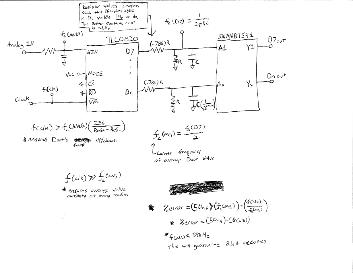
Will the following control set up work?

Thanks

Tony.

  • Tony,

    Is the host receiving the ADC output a microprocessor or a CPLD/FPGA? It is not clear to me how do you intent to qualify the data valid, without any other signal?

    I would recommend using the write-read mode in stand-alone operation as shown in Figure 4 of the datasheet.

    With MODE held high, you should tie both /CS and /RD to low and drive /WR from the 10kHz timer output. In ta(INT) = 50ns max after /INT going low, the ADC will drive valid data on the D0-D7 pins of the device. This can be qualified at the host in one of two ways:
    1. If the /INT output from the ADC is delayed using logic gates by greater than ta(INT), this delayed /INT can be used to qualify the data at the host.
    2. Assuming a 50% duty cycle on the 10kHz output of the timer, the falling edge of /WR can be used to qualify the valid data at the host.

    Regards,
    Sandeep
  • So the output of the ADC is going to a data bus, via card slot.


    I want the card w/ with the ADC to operate continuously without any command from the data bus or require any work from the master controller.

    For this application whether the data available is the most valid or not does not matter. Its for long term monitoring; +/- 500ms would still be no big deal.


    I see figure 4, that is much simpler than what I have... But the DataSheet says on pg9 (/INT pin) that:

    "INT is reset by the rising edge of either RD or CS."

    That is why have /RD pin also in my logic control circuit...

    In this a typo for the /INT pin?

    Thanks
    Tony.
  • Hi Tony,

    The comment regarding the /INT pin is not a typo.  However, operating in Stand-Alone mode per Figure 4, the /CS and /RD pins are always tied low, so the /INT pin will only toggle high/low relative to the rising edge of the /WR pin.

    Also note that the min/max pulse width of /WR is 0.5uS to 50uS.  At 10kHz, 50% duty cycle, you will be at the max limit of 50uS for the /WR timing.  I suggest running the duty cycle of the clock connected to the /WR pin at 60% duty cycle or more in this case.  Per the previous post, you will then be guaranteed valid data at the falling edge of the /WR pin and data will remain valid during the entire time that /WR is low.

    If you do read the data outputs asynchronously to the /WR pin (or /INT pin) per Figure 4, just keep in mind that a percentage of the readings will be corrupted, which will occur when the Dout pins are toggling between conversion results.

    Regards,
    Keith N.
    Precision ADC Applications

  • Hmm.


    Could I tie a D-Latch to the delayed /INT signal? Would that prevent invalid data from getting onto the Bus, or would have the same problem with the added D-Latch?


    Or have capacitive LPF loads on a secondary buffer/D-Latch, which would filter out any sudden bit toggles?
  • When the output is updated, each of the bits will transition with slightly different time delays. If the Dout's of the TLC0820A are transitioning at the exact moment that your system is reading them, then you will get corrupted data. Think of this as a settling time on the digital outputs. Once settled, the data will be valid. If your system reads the same conversion result a second time, then you would get valid data. Since you are only taking samples every 100uS, I suggest reading the data multiple times in succession at ~1uS intervals and then use a 'voting' count to determine the correct reading.
  • Tony,

    Adding a D-Latch such as the SN74HCT373 on the D0-D7 bus, qualified by a flipped and delayed /INT should ensure stable data on the bus.

    Regards,

    Sandeep

  • Ugh, I wish I read that this morning... That's how I will do it.

    Its meaningless now but I came up with a nifty Digital Low Pass filter design that would have also solved the invalid data problem.

  • Regarding the D-Latch...

    Would an ACT or ABT type Latch also work or is the HCT type ideal?

    In the TI Logic guide, for HCT it says:

    "Balanced propagation delay and transition

    times"

    Is this what prevents invalid data being read during transition... e.i. all outputs will switch at the same time?

    Thank you

    Tony

  • Hi Tony,

    Any of these parts should work well.  This will guarantee that the data is stable throughout the entire conversion process.

    Regards,
    Keith N.