


Other Parts Discussed in Thread: LMP90080, ADS124S08, ADS1248, LMP90100
Hi team
can I get your reply ?
[1] I need to calculate TUE.
For worst TUE after calibration, I used INL = 1LSB, Offset = 15uV, Offset drift = 100nV/⁰C, Gain = 100PPM,
and Gain drift = 0.5PPM/⁰C with Max Ta = 150⁰C,
And finally, I found TUE is 0.826[mV]( = 5.418[LSB]).
By using any one of BgcalMode1/BgcalMode2/BgcalMode3 without using system calibration,
Lmp90080 can meet TUE is 0.826[mV]( = 5.418[LSB]) that I calculated for worst case ?
We will not use system calibration.
[2] at the condition that don’t use system calibration and background calibration also,
Customer wants to calculate TUE. What data(INL/Offset/Offset drift/Gain/Gain drift) I have to use for the calculation ?
[3] in the middle of running any one of BgcalMode1/BgcalMode2/BgcalMode3,
Any time we can execute system calibration ?
[4] under disabling background calibration,
If we run system calibration just only one time, such the one time calibrated offset & gain will be used forever ?

[5] what is the purpose of post calibration ?
I cannot understand why I need it and how to use it.
I need more explanation on SCAL_SCALING and SCAL_BITS_SELECTOR.
[6] for system calibration, CH0 ~ CH3 have their offset and gain registers by actual board level calibrated.
CH4 ~ Ch6 will reuse the offet and gain of CH0 ~ CH2 respectively.
So, I think the accuracy for CH4 ~ CH6 might be not best because they don’t have their actual calibrated result.
That means, at single ended ADC, customer would better to use only 4 channels for CH0 ~ CH3 among total 7 channels
by CH0 ~ CH6.
How about your view on my that point ?
Or, can we ensure IC can secure still best accuracy even for CH4 ~ CH6 at using total 7 channels single ended ADC ?
[7] for system calibration, CH0 ~ CH3 have their offset and gain registers by actual board level calibrated.
CH4 ~ Ch6 will reuse the offet and gain of CH0 ~ CH2 respectively.
How about background calibration which also have each offset and gain registers for CH0 ~ CH3,
And will reuse the offet and gain of CH0 ~ CH2 for CH4 ~ CH6 ?
[8] at system calibration, IC needs system zero-scale condition and system reference scale condition for offset & gain calibration.
(8-1) for single ended ADC channel, Is it OK for me to select any output code among the lower Vin range for system zero-scale
condition as below, And to select any output code among the higher Vin range for system reference scale condition as below ?
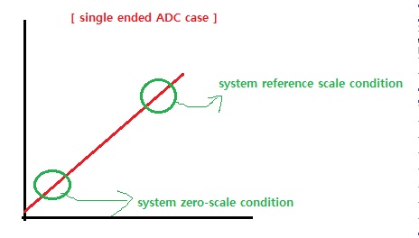
(8-2) for differential ADC channel, Is it OK for me to select any output code among the lower Vin range for system zero-scale
condition as below,
And to select any output code among the higher Vin range for system reference scale condition as below ?

[9] burnout current is used to detect external sensor diagnostic.
My understaning is it can detect external sensor open/short/ and so on.
One sourcing current is from VA to VINP, and the other sinking current is from VINN to GND.
My question is I can enable the burnout current for external sensor diagnostic regardless of differentical ADC or
Single ended ADC ?
For example, normally we uses RC filter for single ended.
I wonder I can use the burnout current feature no matter what the H/W configuraion implemented on VINx pins ?

[10] SHORT_THLD_FALG = 1 means two VINx pins are shorted fault ?
[11] RAILS_FLAG = 1 means one of VINx pins is more than (VA ─ 50mV) ?
[12] about SAMPLED_CH bit.
It means the channel that happens any one of SHORT_THLD_FLAG/RAIL_FLAGS/OFLO_FLAG ?
[13] at ScanMode1/ScanMode2/ScanMode3, how we can know the current read ADC_DOUT is for which channel ?
[14] about DT_AVAIL_B register.
D/S say DT_AVAIL_B = 0 means new ADC conversion is available, and DT_AVAIL_B = 1 means no new ADC conversion ready,
But the register map description is that 0x00 ~ 0xFE means available, and 0xFF means Not available.
Which one is correct ?

[15] DT_AVAIL_B is “Read Only”.
DT_AVAIL_B is cleared when MCU read ADC_DOUT ?
I wonder when the register is cleared.
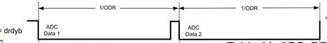
[16] at ScanMode2 with FIRST_CH = CH0 and LAST_CH = CH5, how MCU can correctly know the current ADC_OUT is for which channel ?
[17] at SDO_DRDYB_DRIVER = 00(DrdybCase1 mode), I did read ADC_DOUT completely at SDO/DRDYB pin = low.
Then, how I can make SDO/DRDYB pin go to High again in order to detect the next ADC available ?
[18] at SDO_DRDYB_DRIVER = 03(DrdybCase2 mode), I did read ADC_DOUT completely at SDO/DRDYB pin = low.
Then, how I can make SDO/DRDYB pin go to High again in order to detect the next ADC available ?
Atfer done reading ADC_DOUT, SDO/DRDYB pin go to High automatically ?
[19] for Data Only Transaction, how I can make device to enter the data first mode ?
Table 4 means using INST2 byte setting alone, I can get to data first mode and get out of data first mode ?
Atfer done reading ADC_DOUT, SDO/DRDYB pin go to High automatically ?

[20] by PWRCH = Standby mode, ADC will be aborted. Later, if I set PWRCH = Active mode, IC will resume ADC conversion automativally ?
Or, I have to write RESTART[0] = 1 ?
[21] in the middle of runing ADC conversion with ScanMode2, can I stop and resume ADC by sending RESTART[0] = 0 or 1 ?
If not, how I can stop and resume ADC conversion manually ?
[22] after power-on, I send all ADC necessary registers initilzation such as CH_SCAN/CHx_INPUTCN/CHx_CONFIG.
Then, I has to set RESTART[0] = 1 to run ADC conversion ?
[23] for example, using 3 single ended channels with ODR = 107.325 SPS for all 3 channels, the ODR per channel will be 35.775SPS(= 107.325/3) ?
[24] what about different ODR seting case for each channel ?
For example, using 3 single ended channels with ODR = 107.325 SPS for CH0, ODR = 26.83125 SPS for CH1, and 6.71SPS for Ch2, the ODR per channel will be what ?
[25] what about different ODR seting case for each channel ?
For example, using 3 single ended channels with ODR = 107.325 SPS for CH0, ODR = 26.83125 SPS for CH1, and 107.325SPS for Ch2, the ODR per channel will be what ?
