This thread has been locked.

If you have a related question, please click the "Ask a related question" button in the top right corner. The newly created question will be automatically linked to this question.

PGA970EVM: Precision Data Converters Forum

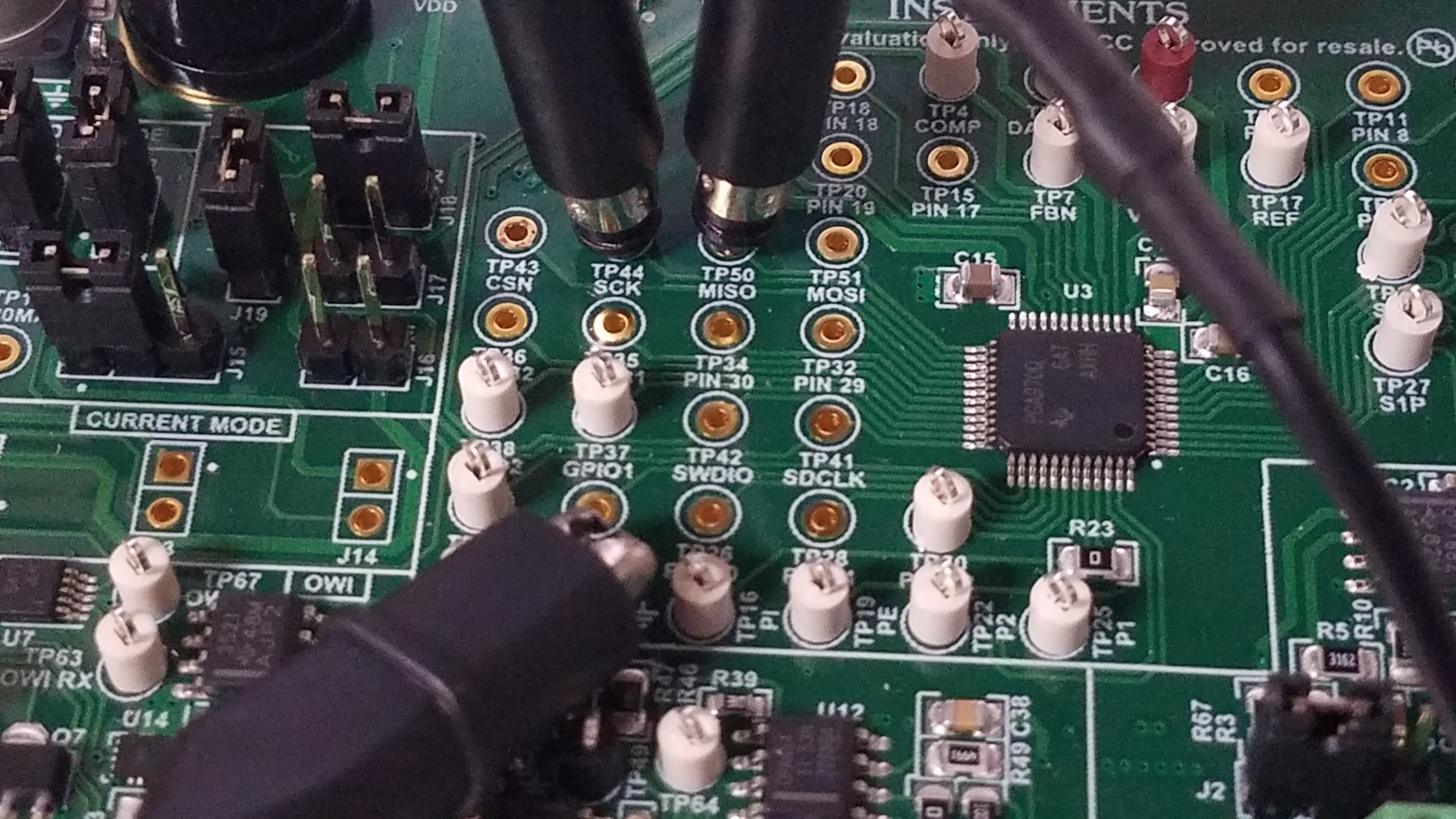
Part Number: PGA970EVM

Using the PGA970GUI and the supplied USB2ANY device for communication with the PGA970EVM.

The PGA970 will not produce any waveform on P1 or P2

I have verified the PGA970 has at least some function by verifying voltage levels and data transfer:

7.5-V, 5-V, and 3.3-V regulators all within 10%

The AVDD and DVDD are also within 10%

I connected an oscilloscope to MOSI and MISO using SPI to communicate, load the FRAM and press Verify FRAM, there is data to and from the PGA970 on pins MOSI and MISO.

When I press Verify FRAM and the FRAM Status gets to 100% the NOT MATCHED "LED" never changes.

I followed the settings found in the PGA970EVM manuals for the ADC settings as well as recommended settings found on ti E2E threads related to the PGA970.

The waveform generator will not produce an output.

measuments are taken related to TP23 ground

when I enable VREF Buffer, the voltage on pin P1 will go from 60mv to 1.8 volts DC and on pin P2 will go to 1.08 volts DC.

the Analog Power has no effect on the P1 and P2

the settings, GAIN_CTRL, SEM, DAC_VCM, DIFF_VOCM all have an effect the DC voltage on pins P1 and P2 a small amount

example:

  • GAIN_CTRL = 1                 P2 = 1.08vdc
  • GAIN_CTRL = 1.67            P2 = .840vdc

MICRO_RESET also has no effect on the P1 and P2 outputs

I removed the jumpers J2 and J7 to verify the LVDT primary is not loading the circuit.

I have verified that I can write to the registers of the MCU by dumping FRAM an DEVRAM also reading the Data & Waveform RAM

Nothing I have tried will produce a wave form, only DC on P1 and P2

mesuements taken related to TP45 ground, P1A and P2A are at 9.2 volts DC

  • I am not using CCSV8 now that you have explained to me I need an XDS200

    Debug is not what I am after.

    I am using the PGA970GUI to communicate with the PGA970EVM now.

    I am unable to get the waveform generator to operate.

    The only thing I can see wrong is when  I press Verify FRAM and the FRAM Status gets to 100% the NOT MATCHED "LED" never changes.

    do you believe the PGA970 on this EVM board is damaged?

    Jaime

  • Hi Jaime,

    Thanks for the detailed description of your testing. The first check will be to make sure the PGA970 device and EVM are working properly, and this should be done with the MCU in reset.

    When you adjusted the GAIN_CTRL, SEM, etc. settings, was this done with the GUI? Or through your firmware?

    If it was done through the GUI, then you are required to place the MCU in reset to reach the ADC settings page where the waveform generation section is (otherwise the GUI will not let you navigate to the ADC settings page). The GAIN_CTRL, SEM, DAC_VCM, DIFF_VOCM, and WFM Bias settings on the GUI will all take effect immediately regardless of whether the waveform data table has been populated, and they will affect the DC output of the P1 and P2 pins. In order to produce a sine output, you will need to set the desired WFM amplitude and WFM frequency, then click the "Populate Waveform Table" button. This will only populate the table in the GUI and will not automatically write the waveform data to the PGA970. Once you click the "Write" button below the data table, the PGA970 will be ready to generate the output waveform. Click the "Generate" button and you should see a sine output on P1 and P2.

    Full instructions for this are included in the GUI user's guide under the ADC settings section: www.ti.com/.../sldu023.pdf

    Is the HEX file you are loading into the FRAM the original file included with the PGA970 generic firmware, or have you modified the firmware and recompiled to generate a new HEX?

    Regards,
  • Mr. Cummins

    I am using the GUI.
    The firmware was not modified.
    I downloaded the PGA970_FW_Release_1_5_Generic hex
    With no modification, that file was loaded into the FRAM.
    The Not Matched "LED" never changes after pressing Verify FRAM.
    After setting the WFM A to 375mv and WFM F to 5kHz, I pressed Populate Waveform Table.
    Then I pressed Write
    I connected my scope leads:
    • reference ground clip to TP23
    • channel 1 probe clip to TP25
    • channel 2 probe clip to TP22
    • set vertical amplitude on the scope to 500mv per div.
    After the Write Status finished, I pressed Generate.
    There is no waveform generated on P1 or P2.
    The LVDT device connected is an RDP GTX1000
    https://www.rdpe.com/us/gt.pdf
    Do I need to ask for an RMA to send in the PGA970EVM for evaluation?

    Jaime
  • Hi Jaime,

    Can you please save your register map to a file in the Low Level Configuration page and post it here (place the MCU in reset and read all before saving)? 

    Also, I am attaching a hex file that writes all zeros to the memory space. Please try to load this into the FRAM. It will not fill the full 16kb, but the generic firmware takes up less than 8kb, so the zeros should cover it. Please verify the load afterward and check that the light changes to "Matched"

    pga970_fram_allz_8k.hex

    I need to do some testing on my end to help troubleshoot before we move to an RMA, but it is a possibility that your EVM is defective. I'd just like to rule out some other things first.

    Regards,

  • the light did not change to "Matched"

    BTW
    I noticed the USB connection had a potential problem..
    The green LED on the USB2ANY would flash before.
    this time when i connected the interface disconnected message would cycle with the USB connection detected message.
    I noticed the cable to the USB may not have been pressed in well on the port of the PC.
    after correcting this, I restarted the PC, then the GUI before attempting the procedures you recommended.
    this did not happen before.
  • LLC 0s.cfg   this is the Low Level Configuration with all zeros loaded

  • Looking at the FRAM dump helped me understand the addressing.
    First column is the page address
    Second column is the word address
    Third column is the value of the data in hex located in the 8 bit word at that address.

    an amateur question, but is this correct?
  •    please notice the attached photos taken when loading FRAM

    yellow is data

    blue is SCK

    1st is MOSI

    2nd is MISO

  •  Showing my amateur skill level again.....

    maybe this photo is a little better....

    channel 1 is MOSI

    channel 2 is MISO

    channel 3 is SCK

  • Hi Jaime,

    Your assumption about the structure of the HEX file is correct. Looking at the two FRAM dumps you sent, it certainly seems like the device is not being programmed at all when you load the HEX file through the GUI.

    The final thing I can think of that may be preventing the programming is the security lock for the FRAM. In the low level configuration files you sent me, the SECLOCK register is 0h00, which means it is unlocked. However, before you try to program just make sure that is the case.

    What voltage do you supply to the power inputs for the EVM?
  • Hi Jaime,

    Thanks. I think something may be wrong with your board. Someone already contacted me about the RMA, so we can get that approved.

    Regards,
  • Thank you Mr. cummins, I will look forward to receiving the unit back to me verified functional or repaired so I can continue learning about the unit, then develop my application.
    The SECLOCK bit is definitely = 0
    I noticed SECLOCK when I was reading through the PGA970 pdf file.
    The diagnostics procedures I did prompted me to learn a lot about this device that would have otherwise taken me much longer.
    I explored the documentation I have covering the device, probing voltages, and signals.
    The logic I was using is that data pulses on the MISO that indicate the MCU was answering the USB2ANY.
    Does this prove the MCU is running.?
    I will await the communication from sales.
    Have a great day!