Part Number: DAC3482EVM
DEARS.
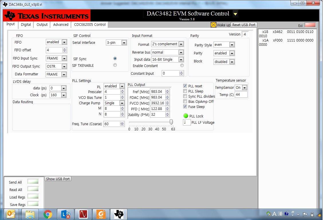
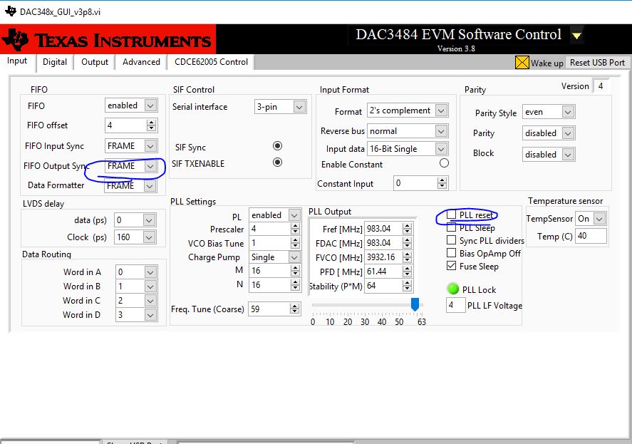
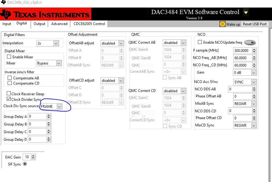
I operated EVM in external mode.
How can I use internal PLL to drive DAC3482EVM?
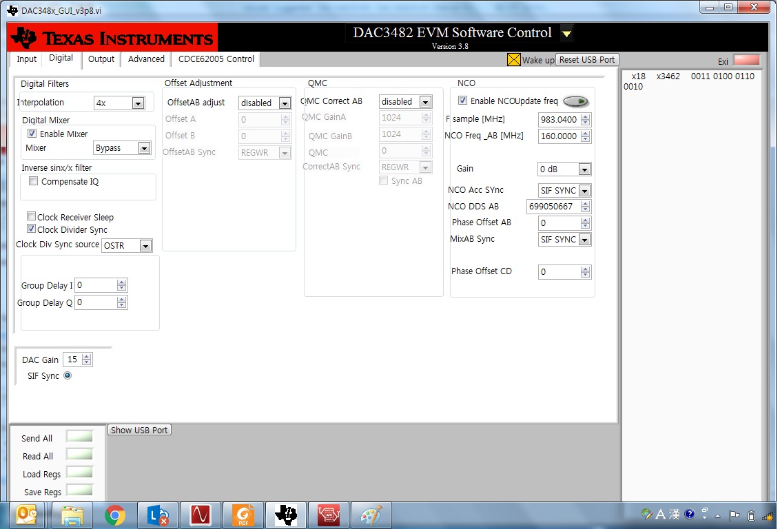
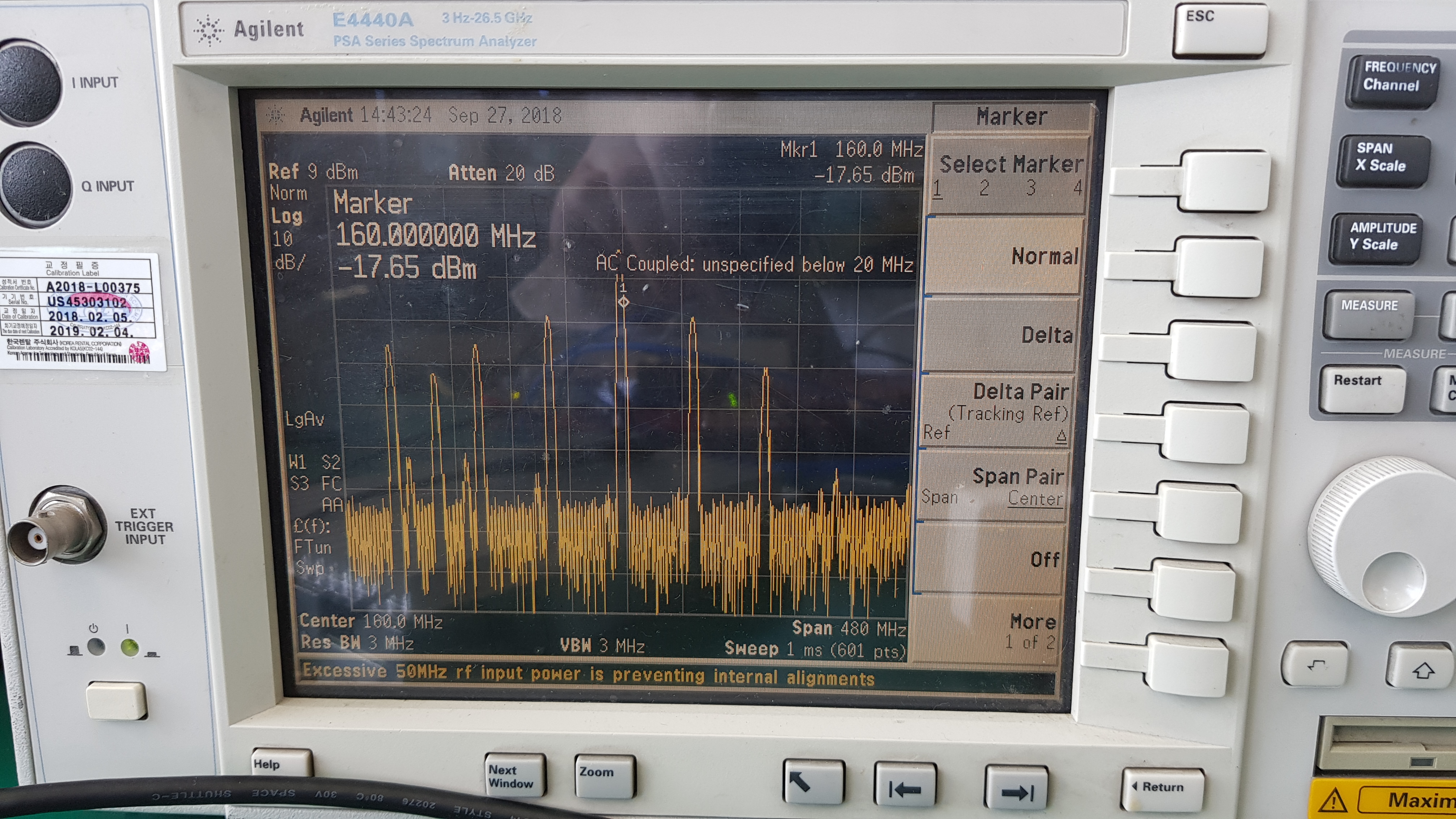
Clock : 245.76Mhz x 4(interpolation),
interpolation : x4
Internal PLL is used.
Thank you.
Part Number: DAC3482EVM
DEARS.
I operated EVM in external mode.
How can I use internal PLL to drive DAC3482EVM?
Clock : 245.76Mhz x 4(interpolation),
interpolation : x4
Internal PLL is used.
Thank you.