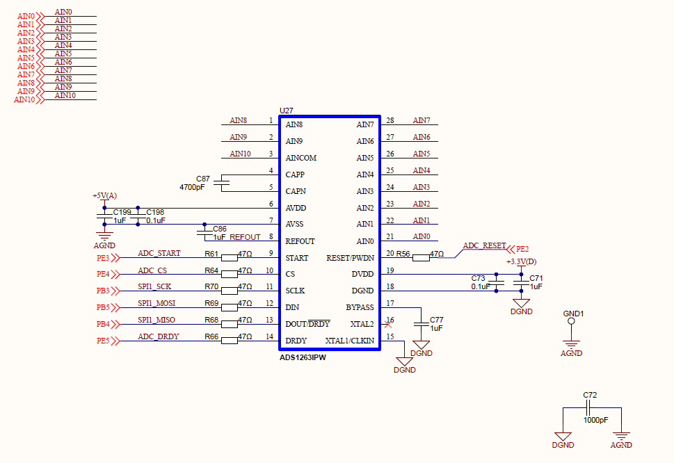
Part Number: ADS1263
Other Parts Discussed in Thread: ADS1262
as suggest by Chris, I go ahead but nothing get resolved. Issue is still there basic problem from my point of view when I see the example given by TI
- How to configure that which ADC get initialized and where to read its data as ADC had 11 channels no. in it
- no timing diagram is provided in data sheet (this definitely give easy way to us to know its working)
- i had done some initialization and as below but don't know where the issue is
////////////////////////// INCLUDE FILE ////////////////////////////////////////
#include "ADS1263.h"

////////////////////////// PIN DECLARATIONS ////////////////////////////////////
sbit defADC1263_RESETPin   at GPIOE_ODR.B2;
sbit defADC1263_STARTPin   at GPIOE_ODR.B3;
sbit defADC1263_CSPin      at GPIOE_ODR.B4;
sbit defADC1263_DRDYPin    at GPIOE_ODR.B5;

sbit defADC1263_SCKPin     at GPIOB_ODR.B3;   //
sbit defADC1263_DOUTPin    at GPIOB_ODR.B4;   //
sbit defADC1263_DINPin     at GPIOB_ODR.B5;   //

char j;

/*
  ADS1262.h - Library for ADS1262 Shield Arduino Firmwar.
  Created by Protocentral, December 27, 2013.
  Released into the public domain.
*/
char* ads1262_Read_Data(){
    static char SPI_Dummy_Buff[6];
    defADC1263_CSPin_Clr;

    for (j = 0; j < 6; ++j){
        SPI_Dummy_Buff[j] = SPI3_Read (CONFIG_SPI_MASTER_DUMMY);
    }
    defADC1263_CSPin_Set;
    return SPI_Dummy_Buff;
}

void ads1262_Init(){
    GPIO_Digital_Output(&GPIOB_BASE, _GPIO_PINMASK_3 | _GPIO_PINMASK_5);
    GPIO_Digital_Output(&GPIOE_BASE, _GPIO_PINMASK_2 | _GPIO_PINMASK_3 | _GPIO_PINMASK_4);
    GPIO_Digital_Input (&GPIOE_BASE, _GPIO_PINMASK_5);
    GPIO_Digital_Input (&GPIOB_BASE, _GPIO_PINMASK_4);

//defADC1263_RESETPin_Set;
//defADC1263_STARTPin_Set;
//defADC1263_CSPin_Set;
//defADC1263_SCKPin_Set;
//defADC1263_DINPin_Set;
//while(1);
    // start the SPI library:
//    SPI.begin();
//    SPI.setBitOrder(MSBFIRST);
    //CPOL = 0, CPHA = 1
//    SPI.setDataMode(SPI_MODE1);
    // Selecting 1Mhz clock for SPI
//    SPI.setClockDivider(SPI_CLOCK_DIV8); // DIV16

    // hs
//    SPI2_Init();

SPI3_Init();
    ads1262_Reset();
    Delay_ms(100);
    // ads1262_Disable_Start();
    // ads1262_Enable_Start();

    ads1262_Hard_Stop();
    // ads1262_Start_Data_Conv_Command();
    // ads1262_Soft_Stop();
    Delay_ms(50);
    //  ads1262_Stop_Read_Data_Continuous();                                        // SDATAC command
    Delay_ms(300);

    ads1262_Reg_Write(POWER, 0x11);                 //Set sampling rate to 125 SPS
    Delay_ms(10);
    ads1262_Reg_Write(INTERFACE, 0x05);        //Lead-off comp off, test signal disabled
    Delay_ms(10);
    ads1262_Reg_Write(MODE0, 0x00);                //Lead-off defaults
    Delay_ms(10);
    ads1262_Reg_Write(MODE1, 0x80);        //Ch 1 enabled, gain 6, connected to electrode in
    Delay_ms(10);
    ads1262_Reg_Write(MODE2, 0x06);        //Ch 1 enabled, gain 6, connected to electrode in
    Delay_ms(10);
    ads1262_Reg_Write(INPMUX, 0x01);        //Ch 1 enabled, gain 6, connected to electrode in
    Delay_ms(10);
    ads1262_Reg_Write(OFCAL0, 0x00);        //Ch 1 enabled, gain 6, connected to electrode in
    Delay_ms(10);
    ads1262_Reg_Write(OFCAL1, 0x00);        //Ch 1 enabled, gain 6, connected to electrode in
    Delay_ms(10);
    ads1262_Reg_Write(OFCAL2, 0x00);        //Ch 1 enabled, gain 6, connected to electrode in
    Delay_ms(10);
    ads1262_Reg_Write(FSCAL0, 0x00);        //Ch 1 enabled, gain 6, connected to electrode in
    Delay_ms(10);
    ads1262_Reg_Write(FSCAL1, 0x00);        //Ch 1 enabled, gain 6, connected to electrode in
    Delay_ms(10);
    ads1262_Reg_Write(FSCAL2, 0x40);        //Ch 1 enabled, gain 6, connected to electrode in
    Delay_ms(10);
    ads1262_Reg_Write(IDACMUX, 0xBB);        //Ch 1 enabled, gain 6, connected to electrode in
    Delay_ms(10);
    ads1262_Reg_Write(IDACMAG, 0x00);        //Ch 1 enabled, gain 6, connected to electrode in
    Delay_ms(10);
    ads1262_Reg_Write(REFMUX, 0x00);        //Ch 1 enabled, gain 6, connected to electrode in
    Delay_ms(10);
    ads1262_Reg_Write(TDACP, 0x00);        //Ch 1 enabled, gain 6, connected to electrode in
    Delay_ms(10);
    ads1262_Reg_Write(TDACN, 0x00);        //Ch 1 enabled, gain 6, connected to electrode in
    Delay_ms(10);
    ads1262_Reg_Write(GPIOCON, 0x00);        //Ch 1 enabled, gain 6, connected to electrode in
    Delay_ms(10);
    ads1262_Reg_Write(GPIODIR, 0x00);        //Ch 1 enabled, gain 6, connected to electrode in
    Delay_ms(10);
    ads1262_Reg_Write(GPIODAT, 0x00);        //Ch 1 enabled, gain 6, connected to electrode in
    Delay_ms(10);
    ads1262_Reg_Write(ADC2CFG, 0x00);        //Ch 1 enabled, gain 6, connected to electrode in
    Delay_ms(10);
    ads1262_Reg_Write(ADC2MUX, 0x01);        //Ch 1 enabled, gain 6, connected to electrode in
    Delay_ms(10);
    ads1262_Reg_Write(ADC2OFC0, 0x00);        //Ch 1 enabled, gain 6, connected to electrode in
    Delay_ms(10);
    ads1262_Reg_Write(ADC2OFC1, 0x00);        //Ch 1 enabled, gain 6, connected to electrode in
    Delay_ms(10);
    ads1262_Reg_Write(ADC2FSC0, 0x00);        //Ch 1 enabled, gain 6, connected to electrode in
    Delay_ms(10);
    ads1262_Reg_Write(ADC2FSC1, 0x40);        //Ch 1 enabled, gain 6, connected to electrode in
    Delay_ms(10);
     ads1262_Start_Read_Data_Continuous();
    Delay_ms(10);
    ads1262_Enable_Start();
}

void ads1262_Reset(){
    defADC1263_RESETPin_Set;
    Delay_ms(100);                                        // Wait 100 mSec
    defADC1263_RESETPin_Clr;
    Delay_ms(100);
    defADC1263_RESETPin_Set;
    Delay_ms(100);
}

void ads1262_Disable_Start(){
    defADC1263_STARTPin_Clr;
    Delay_ms(20);
}

void ads1262_Enable_Start(){
    defADC1263_STARTPin_Set;
    Delay_ms(20);
}

void ads1262_Hard_Stop (void){
    defADC1263_STARTPin_Clr;
    Delay_ms(100);
}


void ads1262_Start_Data_Conv_Command (void){
    ads1262_SPI_Command_Data(START);                                        // Send 0x08 to the ADS1x9x
}

void ads1262_Soft_Stop (void){
    ads1262_SPI_Command_Data(STOP);                   // Send 0x0A to the ADS1x9x
}

void ads1262_Start_Read_Data_Continuous (void){
    ads1262_SPI_Command_Data(RDATAC);                                        // Send 0x10 to the ADS1x9x
}

void ads1262_Stop_Read_Data_Continuous (void){
    ads1262_SPI_Command_Data(SDATAC);                                        // Send 0x11 to the ADS1x9x
}

void ads1262_SPI_Command_Data(unsigned char data_in){
    char cdata[1];
    //data[0] = data_in;
    defADC1263_CSPin_Clr;
    Delay_ms(2);
    defADC1263_CSPin_Set;
    Delay_ms(2);
    defADC1263_CSPin_Clr;
    Delay_ms(2);
    SPI3_Write (data_in);
    Delay_ms(2);
    defADC1263_CSPin_Set;
}

//Sends a write command to SCP1000
void ads1262_Reg_Write (unsigned char READ_WRITE_ADDRESS, unsigned char DATA){
    char dataToSend;
    // now combine the register address and the command into one byte:
    dataToSend = READ_WRITE_ADDRESS | WREG;

    defADC1263_CSPin_Clr;
    Delay_ms(2);
    defADC1263_CSPin_Set;
    Delay_ms(2);
    // take the chip select low to select the device:
    defADC1263_CSPin_Clr;
    Delay_ms(2);

    SPI3_Write (dataToSend); //Send register location
    SPI3_Write (0x00);                //number of register to wr
    SPI3_Write (DATA);                //Send value to record into register

    Delay_ms(2);
    // take the chip select high to de-select:
    defADC1263_CSPin_Set;
}

char ADCS_DRDY_Status(){
    char ucStatus;
    if(defADC1263_GetPinStatusDRDY == 0)               // monitor Data ready(DRDY pin)
    {
        ucStatus = 1;
    }
    else {
        ucStatus = 0;
    }
    return ucStatus;
}
There is some ADS1263 example code that was released along with the TIPD188 reference design. Please, refer to the "TIPD188 Firmware" download, under the "Software" section. I hope that helps you out!

Best regards,
Chris