Part Number: ADC12J4000EVM
Other Parts Discussed in Thread: ADC12J4000
Hello,
we have bought an ADC12J4000 EVM and are currently working with Xilinx VC707 firmware (TI_HSDC_Pro_Reference_design_V2.8), as a base for our own development of a simpler firmware.
Our current task is interpreting the data received from our ADC Platform, and, while implementing my own firmware, we noticed a perplexing behaviour regarding the ordering of each sample.
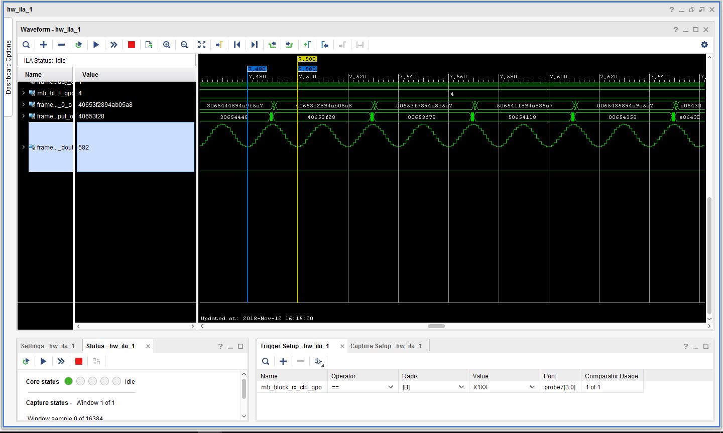
To test it out, we have set up the Ad converter to transmit in TEST PATTERN MODE and watch the results (as in SLAS989D, table 33, page 48).
In the attached image we have the rx_tdata (input to the data_block of the sample firmware) and the test pattern data as in your manual.
We Expected a certain behaviour, but:
- we recognized that each half byte is inverted
- we recognized that bytes are inverted in couples
- what we are missing is the correspondence of the byte which should be the LSB of samples number 16-17-18-19-20-21-22-23 as in the table 13 of the aforementioned SLAS989D document.
What are the bytes in red colour actually representing?
Are we extrapolating the data in the wrong position?