This thread has been locked.

If you have a related question, please click the "Ask a related question" button in the top right corner. The newly created question will be automatically linked to this question.

ADS122U04: ADS122U04

Part Number: ADS122U04
Other Parts Discussed in Thread: ADS1220, , ADS124S06, ADS1219

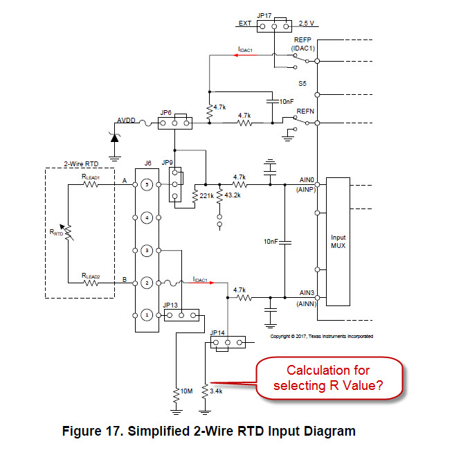
Hello I have a question on the schematic for the ADS122U04 EVM.  For the setup for a 2-Wire RTD that is shown below there is a Resistor in the schematic R79 shown below as a 3.4K value resistor.  The EVM User Manual indicates that this may need to be changed depending on the iDAC output current and R77 Value(4.7K on the EVM) that creates the VREF voltage.  It is not clear how to determine an appropriate value for R79 based on changes that would be made to the IDAC output current and hence updated R77 value to create the desired VREF voltage?

Can someone please assist with the calculation to determine the correct value and also help with the understanding of the purpose of this resistor?  The notes in Sect 5.1.1 of the EVM manual indicate R79 is to maintain proper common mode voltage when using the PGA gain but I am not really clear on my understanding of this.  I understand what Common-Mode is and the PGA requirements for this.

My specifics are

Using the ADS1220

IDAC = 10 or 50uA depending on our specific NTC Thermistor

AVDD = 3.3V though may need to bump this up higher to accomodate IDAC compliance.

Any insight would be very helpful and welcomed...

Regards,

Frank

  • I should also add that I am currently planning on the following parameters...
    IDAC = 50uA
    R77/R78 = 48K to generate a 2.4V VREF

    In the EVM schematic R75(4.7K) AIN3 input Resistor is also matched to R77/R78. Should I be matching an input Resistance with the R77/R78 values and adjust the Cap value accordingly to maintain a similar RC LPF? I believe the R75 value is more to do with the input RC filter than matching the R77/R78 values but not 100% sure?

    Regards,
    Frank
  • Hi Frank,

    The ADS122U04EVM uses a high-side reference for making ratiometric measurements.  There is an RTD measurement guide with useful information and descriptions that can be found at:

    http://www.ti.com/lit/pdf/sbaa275

    The 3.4k resistor is used for biasing the input voltage to the correct common-mode input range for the PGA.  In general you want to target around mid-AVDD supply for setting the sensor common-mode.  The reference resistor needs to be large enough to establish at least 0.5V (minimum external reference input) for the IDAC current being used.  The total voltage drop of the IDAC current path must meet the IDAC compliance voltage (AVDD-0.9V) to maintain constant current.

    The circuit shown is for an RTD, but you are later describing a thermistor.  Without knowing the thermistor resistance range of the temperature range being measured it is a little more difficult to give specific resistor values.

    Best regards,

    Bob B

  • Hi Bob,
    Maybe a different way to ask this same question is lets take the exact same scenario that is described in the ADS122U04 EVM User Guide for the 2 Wire RTD.

    PT100 RTD
    IDAC = 250uA
    R77 = 4.7K

    Can you describe how the 3.4K value of R79 was derived and how the Common-Mode Voltage is derived from this 3.4K value?

    Regards,
    Frank
  • Where I am not clear is how to treat the IDAC current being split between the 4.7K input resistor and then the 3.4K Bias resistor. I.E. - Should it be assumed that the ADC input is HIGH IMPEDANCE and the current primarily just goes through the 3.4K resistor to create the Common Mode voltage? OR???

    Frank
  • Hi Frank,

    Our posts overlapped. The only resistor values you need to change are R78 and R79. The other resistors are used for current limiting and noise filtering to the ADC inputs.

    2.4V reference is too large unless you plan on using 5V for AVDD. Calculate the largest thermistor resistance and work from there. What is your largest thermistor resistance value?

    Best regards,
    Bob B
  • Hi Frank,

    We keep sending at the same time. The ADC input is high impedance. Consider this input to be nAs worst case. The IDAC current path is through the reference resistor (R78), through the sensor and finally through R79 to AGND.

    3.4k for R79 is based on 3-wire RTD which will have 250uA + 250uA flowing through R79. This will come out to about 1.7V for biasing the sensor common-mode when using 3.3V AVDD (approximately mid-AVDD in this case). It will be about 0.85V for the 2-wire case. The key here is if the PGA is enabled and used, even at a gain of 1 the AIN3 input must be at least 200mV above AGND.

    Hope this makes more sense.

    Best regards,
    Bob B
  • Hey Bob Thanks for all the replies. Yeah after reading the RTD Guide you provided the link for I am realizing I need to set a VREF somewhere around 1.65V as it stands right now with an AVDD = 3.3V. The particular Thermistor for this design has not solidified but from some first hand calculations last night working with AVDD = 3.3V it appears that the following could work fairly well...

    NTC
    10K @ 25deg C
    B25/B85 = 3435
    IDAC = 10uA

    Yields
    R-40 = 248,277ohm : Vinput = 2.48 G=1
    R105 = 874ohm : Vinput=8.74mV G=1 ; 1.12V G=128

    Am I heading in the right direction?? Does this give you a better feel for my prior questions on calculation of R79? Still just not sure how to evaluate the Voltage that R79 generates? I.E. - Should all the IDAC current be assumed to go through R79 to derive the Vcm it will create? If not how do we consider the IDAC current that would flow into the ADC itself through R75?

    Regards,
    Frank
  • Hi Frank,

    Consider all current going through R79. There is a very tiny bias current going into the ADC, but this is so small in comparison to IDAC current, you can ignore this for the calculation.

    I'm not sure I fully follow your calculations. Essentially you want to make a ratiometric measurement where the code of the ADC relates to the ratio of the thermistor to the reference resistor. You can do this as the IDAC current is common to both. One code (LSB) relates to the full-scale range (FSR) of the ADC and the total available counts. FSR = +/-VREF/GAIN/(2^24 - 1) where VREF is Rref*IDAC. The voltage of the sensor is Rtherm*IDAC. Rtherm = Rref (ADC result)/(2^23)/GAIN.

    R79 is not a part of the conversion calculation. Its sole purpose is to lift (or bias) the sensor into the proper common-mode input range for the PGA if enabled.

    Best regards,
    Bob B
  • Hi Frank,

    let me help out here while Bob is enjoying his time off. I realized this answer got a little long.

    If you only worry about thermistor measurements (or 2-wire RTD measurements) I would actually recommend using a solution where the reference resistor is placed on the low-side of the thermistor. This will make things much easier.

    On the ADS122U04EVM we are using a high-side reference resistor (=R77). This implementation is often preferable to measure 3-wire RTDs because it yields slightly better performance.

    For 2-wire and 4-wire RTD, and thermistor measurements there is no real benefit in placing the reference resistor on the high side.

    One disadvantage of the implementation using the reference resistor on the high-side is, that you need a bias resistor on the low-side (R79) to level-shift the signal across the thermistor/RTD into the common-mode voltage range of the PGA. This will also make it more challenging to meet the headroom for the IDAC to work when using a 3.3V supply.

    As Bob mentioned before, the input currents into the ADC inputs are usually negligible. I would not worry about them for now. The potential errors they introduce can be calibrated out using an offset and gain calibration which you might have to do in any case depending on your temperature measurement accuracy requirements.

    So let's come to calculating the value you need to choose for the reference resistor. Let's start by deriving the formula for converting the ADC code into a thermistor resistance value.

    The ADC compares the differential input signal coming out of the PGA with its reference voltage and provides an output code which represents the ratio between the two:
    Code/2^24 = (V_IN * Gain) / (2 * V_REF).

    V_IN is the voltage drop across the thermistor:
    V_IN = I_IDAC * R_Thermistor

    V_REF is the voltage drop across the reference resistor (R_REF):
    V_REF = I_IDAC * R_REF

    With that:
    Code/2^24 = (R_Thermistor * Gain) / (2 * R_REF).

    You can use this relationship to calculate R_Thermistor from the measured ADC code.

    From the datasheet specifications you will see that V_IN <= V_REF / Gain, or in other words R_Thermistor <= R_REF / Gain.
    For thermistor measurements you usually use Gain = 1 actually. This means that your R_REF needs to be larger than the largest thermistor value you want to measure. In your case 248kOhm I guess.
    With that we would start by choosing R_REF = 250kOhm for example (or something close but at least larger than 248kOhm).

    With an I_IDAC = 10uA, this would yield a reference voltage of 2.5V. This will not work out with a 3.3V supply. Means we definitely need to switch to a 5V supply, but as we will see in a bit this will also not work.
    Using AVDD = 5V, I_IDAC = 10uA and R_REF = 250kOhm, the maximum differential voltage across the thermistor would be 2.48V.
    R_REF and R_Thermistor are in series (no matter if we use the low-side or high-side R_REF approach), means we will create a voltage drop of (2.5V + 2.48V) = 4.98V across the two resistors at T=-40°C. This will leave no headroom for the IDAC to operate anymore.

    The conclusion would be that a 10kOhm NTC measurement down to -40°C using current excitation is not possible with ADS1220/ADS122U04 because we do not offer small enough IDAC values.
    You would therefore have to choose a voltage excitation method which most customers anyway do for thermistor measurements.

    There are multiple ways to do this. The ADS124S06 for example offers a very convenient way of doing it, because this ADC offers a buffered 2.5V voltage reference output which could be used to excite the thermistor. Below is how the circuit would look like (not showing any RC filters on the inputs).

    I typically use the following formula to find the best value for R_BIAS:
    R_BIAS^2 = R_Thermistor_Min * R_Thermistor_Max = 874Ohm x 248.277kOhm

    In your case that would mean setting R_BIAS = 15kOhm.

    The relationship to calculate the thermistor value from the output code would read the following:
    Code/2^24 = (V_IN * Gain) / (2 * V_REF).

    We would use Gain = 1 again here and for V_IN use the following resistor divider equation:
    V_IN = V_REF x R_Thermistor / (R_Thermistor + R_BIAS)

    This yields:
    Code/2^23 =  R_Thermistor / (R_Thermistor + R_BIAS)

    The solution using ADS124S06 will probably offer the best performance. However you can also use cheaper solutions such as ADS1220 or ADS122U04 together with the analog supply (or an external voltage reference) to excite the thermistor. I am describing this solution in the ADS1219 datasheet application section for example.

    Regards,

  • Hi Joachim/Bob,

      Thank You both for your responses.  I wanted to get a quick reply back to let you know I have not disappeared got yanked away onto some other items.  I will be coming back to this topic this week to get a resolve and a solution to move forward with so I may pose a few more questions but from your responses I think I have a handle on this will run by you both what I come up with or have questions with tomorrow...

    Thanks,

    Frank

  • Thanks a lot for the update Frank.

    Keep the questions coming. We are here to help.

    Regards,
  • Hi Frank,

    I haven’t heard back from you. I’m assuming you were able to resolve your issue and I'm going to close out this thread. If you still have an issue, just post a reply below (or create a new thread if the thread has locked due to time-out).

    Best regards,
    Bob B

  • Hi Joachim/Bob,

      So I have come back to this and selected a couple of 10K NTC thermistors that will work well for us.  My question before I submit my schematic to others for review is whether there is any advantage of placing the RBias resistor on Top of the Thermistor vs. below the Thermistor as you have shown?  Seems like whether it is placed on Top or Bottom one still takes the divider measurements in same fashion across the NTC but maybe I am missing something.  Initially I had put the RBias on top of the NTC in which I was planning on using the Load Switch on the AIN3/REFN1 input on the ADS1220 to minimize self-heating in the NTC and also minimze current drain when we are not taking a measurement...

    From the snapshot below TH+_OUT and TH-_IN are the signal paths to a cable that will have the NTC thermistor on the end and TH-_IN is the return path for the signal loop.  

    Anything either of you guys see that should be changed?  I am going to update the R-C filter a bit to reduce the value of R14 to values closer to what you show in the ADS1219 Datasheet.

    Regards,

    Frank

  • Hi Frank,

    it doesn't really matter if the NTC is on the high or low side.
    It also doesn't matter if you measure the voltage with the ADC across the NTC or RREF. It's all just a resistor divider.

    Please remember that you would have to bypass the PGA of ADS1220 or ADS122U04 in your configuration.

    If you wanted to use the PGA to increase the input impedance slightly, you would have to use an excitation voltage which is less than the analog supply of the ADC and then measure differentially across the upper resistor as I have shown in one of my previous figures.
    But I would try your setup first.

    Regarding the RC filter. Please follow my guidelines in the ADS1219 datasheet, section 9.1.4.
    If you don't need the series resistors to protect the ADC inputs from overvoltages, then I would make them relatively small.

    Regards,