This thread has been locked.

If you have a related question, please click the "Ask a related question" button in the top right corner. The newly created question will be automatically linked to this question.

ADS114S06: SPI Communication with ADS114S06

Part Number: ADS114S06

Dear Sir / Madam,

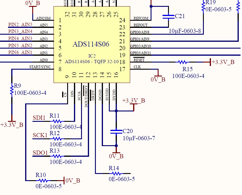
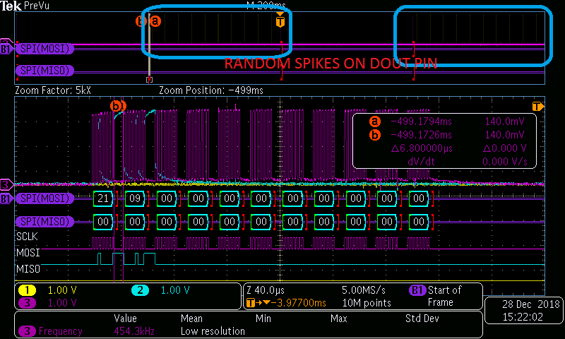
We designed one circuit as suggested in ADS114S06 Datasheet for temperature measurement, but we are unable to reading default Register Data as shown in Register Map.

In controller Program we have set SPI Communication mode-1 (CPOL = 0, CPHA = 1). We are using 8 bit SPI Communication.

Please suggest suitable solution

Thank You.

  • Hi Jehan,

    I'm sorry to hear that you are having trouble with communicating to the ADS114S06. The CPOL=0 and CPHA=1 settings should work, can you verify that you have the proper setup and hold times for the chip select input and that the power supplies are all valid and the device is not being held in reset? Schematics and timing screen shots from an oscilloscope would help us get you going faster.
  • Hi Jehan,

    In addition to Tom's comments, one other very common mistake is not holding CS low throughout the entire communication transaction. If you are using the SS pin for the micro SPI peripheral, this pin will toggle for each byte transmitted. This will cause the communication to cancel. Either control the CS pin of the ADS114S06 with a GPIO holding the CS low throughout the entire communication transaction or tie the CS low.

    Best regards,
    Bob B
  • Hi Tom,

    We are using 3 wire SPI Communication so Only DIN,DOUT & SCLK pins are used from ADS114S06 which is connected to MISO, MOSI, SCLK Pin respectively.

    We are using 8 bit SPI communication where SCLK clock frequency is 460KHz. Only single slave device is available on SPI node so CS pin is connect to GND pin.

    We want to use continuous conversion mode so START/SYNC & RESET pins are connect to 3.3Volt. We are using internal clock of ADS114S06 as clock source so CLK pin is connected at GND.

    And we already checked timing delay between two consecutive queries it is around 10µsec. As per ADS114S06 Datasheet mentioned this time is sufficient.

    Please find attachment circuit diagram below.


    Thank You.

  • Hi Jehan,

    From your description it appears that the SPI connections are incorrect. MOSI (master out slave in) should connect to DIN and MISO (master in slave out) should connect to DOUT of the ADS114S06.

    Best regards,
    Bob B
  • Dear Bob,

    We connect DIN and DOUT pin as you suggested. It was our writing mistake.

    Today we observed random spikes on DOUT pin also.

    Please find attached image of SPI communication waveform for Timing related information , Random spikes observation and Data Received

    from ADS114S06

    Thank You.

  • Hi Jehan,

    If you are tying CS low, then part of the problem is the command needs to timeout as you are not sending enough SCLKs for the command sent. Your command is to read registers starting at register 1, reading 10 registers (as the second byte is the number of registers to be read minus 1).

    Also, many of your digital lines go through resistors or connect to resistors as pullups or pulldowns. I would suggest making sure that all supplies are available at the device pins of the ADS114S06, and reset is pulled high. The device will not communicate if any supplies are missing or if the RESET pin is floating or held low.

    Another method for checking if the ADS114S06 is truly in an operating state is to pull the START/SYNC pin high and monitor DRDY. DRDY should be pulsing at the default data rate. If you do not see this, then the ADS114S06 is not powered or is in a reset condition.

    Best regards,
    Bob B
  • Hi Bob,

    We checked all supply voltage at all pins of ADS114S06, we observed all voltages are sufficient as mentioned in datasheet.

    At present state we observed spikes of 60µSec from DOUT pin of ADS114S06. In previous comment image, you can observe spikes on DOUT pin of ADS114S06.

    Thank You

  • Hi Jehan,

    I have no idea what might be causing the spikes on DOUT. One potential possibility is CS does not have a good connection to ground through the resistor and may actually be floating. Do you have any other devices connected to DOUT? Are there any traces adjacent to DOUT that might be causing a cross talk?

    Did you correct the mistake in your RREG command? You will have continuing issues with trying to read or write to the device if you have incomplete or incorrect commands sent. This might also be causing DOUT to glitch or spike depending on what is being decoded as the command.

    Best regards,
    Bob B
  • Hi Bob,

    There is no any other device connected to DOUT pin. We already Check voltage at CS pin it is GND permanently. 

    We already correct RREG Command, We got correct data too. But spikes of 62µsec is available at every 1.2msec duration. so please suggest us proper solution for this one.

    Thank you.

  • Hi Jehan,

    I was making the assumption that the default settings are being used for the ADS114S06 (single conversion mode at 20sps). Have you attempted to write any of the configuration registers of the ADS114S06? The DOUT/DRDY pin is a dual function pin (see section 9.5.1.4 on page 60 of the datasheet.) The DOUT/DRDY pin will follow the DRDY pin end of conversion period. If the ADS114S06 is configured for Continuous conversions and 800sps you will see the DOUT/DRDY pin transition similar to the manner you have stated. You can verify by placing a scope probe on both DRDY and DOUT/DRDY and you should see the same update period.

    The reason for dual functionality is that in some cases a limited number of inputs to the micro are available and DOUT/DRDY can function as both DOUT and DRDY. A separate DRDY is useful if more than one device is connected to the SPI bus requiring DOUT/DRDY to be high impedance when CS is used. The DRDY is an always active output that can be monitored separately from the SPI communication.

    Best regards,
    Bob B
  • Hi Bob,

    We checked waveform of DOUT/DRDY and DRDY pin. We observed random spikes available on both pin as mentioned above comments.

    Is there any disadvantages or it can make any problems for temperature measurement process?

    Currently we are trying to read ADC Data but we are getting zero value from ADC output.

    All configuration registers are set as per our requirement. All voltages on pin also matched with datasheet mentioned data.

    But still we are getting zero value from ADC output.

    Please suggest us a proper solution for this.

    Thank you.

  • Hi Jehan,

    As the 'spikes' you are seeing relate to end of conversion, this will not affect your measurement.  

    • Can you send me the all the configuration register settings that you are using?  
    • What is connected to the inputs?  
    • And what are you expecting to see as a proper conversion result?  
    • What method of reading the data is being used?  Is it direct or by using the RDATA command?
    • What temperature sensor are you wanting to measure (TC, RTD, etc?)
    • Can you send me scope shots of the communication to read the conversion result?

    One consideration is you should be reading the data after each conversion period ends or there is no advantage of operating the ADC at higher data rates.  Make sure that as soon as DRDY (or DOUT/DRDY) transitions from a high to low state you read the conversion result.  If RDATA is used, this will require 24 SCLKs (RDATA command plus 16 bits of data).

    Once I get the answer to the questions above, I can more accurately answer the question of why you might be seeing a '0' result.

    Best regards,

    Bob B

  • Hi Bob,

    • Our Code flow is as per below sequence 
      • Configure  Micro-controller SPI in Mode-1
      • RESET ADS114S06 by Command 
      • NOP Command
      • 2msec Delay Time
      • WREG Command to set ADS114S06 8 Registers starting from 0x42(Input Multplexer Register) [0x42-0x07-0x12-0x0D-0x14-0x3A-0x00-0xFF-0x04-0x10]
      • Start Command
      • 2msec Delay Time
      • RDATA Command 
      • 2 NOP Command for clocking out data of 16 bit where we get 0x00 result
    • At input side we have connect J type Thermocouple
    • Once writing above registers we checked it using RREG command and to read ADC output value we use RDATA command as mentioned in above sequence
    • We want to measure Thermocouple mV data

    Thank you 

  • Hi Jehan,

    I would suggest reviewing the document 'A Basic Guide to Thermocouple Meaurements':

    http://www.ti.com/lit/an/sbaa274/sbaa274.pdf

    See my comments below.

    Best regards,

    Bob B

    Jehan Patel said:

    Hi Bob,

    • Our Code flow is as per below sequence 
      • Configure  Micro-controller SPI in Mode-1
      • RESET ADS114S06 by Command [BB] This command may not be needed.  The ADS114S06 should come out of a power-on reset (POR) after all the power supplies have reached nominal voltage.
      • NOP Command [BB] This command should not be issued immediately after the RESET command.  Before issuing any further communication with the ADS114S06 after the RESET command, you must wait until the device has fully finished the RESET state.
      • 2msec Delay Time
      • WREG Command to set ADS114S06 8 Registers starting from 0x42(Input Multplexer Register) [0x42-0x07-0x12-0x0D-0x14-0x3A-0x00-0xFF-0x04-0x10] [BB] To recap,you are using AIN1 and AIN2 inputs, PGA enabled with a gain of 32, internal clock, continuous conversions at 20sps and low-latency filter, internal reference which is always on, IDACS off and disabled, VBIAS on AIN2, SPI timeout disabled, no CRC or STATUS byte sent.  As you have tied CS low, there is no way to reset the SPI communication so you might want to consider enabling the SPI timeout feature.  Note that there is some settling delay when you first turn on the internal reference.  See Table 10 on page 34 of the datasheet.
      • Start Command [BB] This command doesn't do any thing as the START pin is pulled high (as shown in the schematic) which will control whether the conversions are running or not.  See section 9.5.3.5 on page 64 of the datasheet.  Note, that the conversions will restart if the configuration registers are changed.  This is discussed in section 9.5.3.12 on page 66 of the datasheet. So the START command is not used if the START/SYNC pin is pulled high.
      • 2msec Delay Time [BB] Conversions are restarted when the WREG command is issued.  At 20sps new data for the first conversion will not be available for 56.504 ms after the WREG command.  See Table 13 on page 40 of the datasheet.  The best method is to monitor DRDY (or DOUT/DRDY) for the high to low transition that signals new conversion results are ready.
      • RDATA Command 
      • 2 NOP Command for clocking out data of 16 bit where we get 0x00 result [BB] I'm not surprised that the first output is all zeros as you have not waited long enough for the conversion to complete before reading it.  If you loop the RDATA command do you always see 0 V output?  It would be very helpful to actually see the RDATA command on a scope or logic analyzer shot.
    • At input side we have connect J type Thermocouple [BB] At room temperature you should see about 475 codes as the output result (or approximately 1.1mV).  This TC should be connected between AIN1 and AIN2.
    • Once writing above registers we checked it using RREG command and to read ADC output value we use RDATA command as mentioned in above sequence [BB]  You should also verify that the reference is operating correctly by measuring 2.5V at the REFOUT pin.  Also verify that VBIAS is ON by measuring approximately 1.65V at AIN2.
    • We want to measure Thermocouple mV data

    Thank you