This thread has been locked.

If you have a related question, please click the "Ask a related question" button in the top right corner. The newly created question will be automatically linked to this question.

ADS1262: Inconsistent /DRDY period (due to poor CLK connection)

Part Number: ADS1262
Other Parts Discussed in Thread: ADS1263, , TIPD188

Hi, I'm very new to TI ADS1263 and I have a problem with reading the data.
If I give AIN0-AIN1 a voltage from 2mV to 15mV I have random data (a kind of high-frequency wave not influenced by the voltage) but if I put a pin on the ground I can see a difference (so I think my ad is "listening").
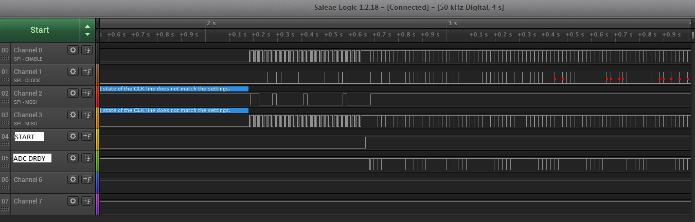
I grounded both AIN0 and AIN1 and checked the signals from a logic analyzer: is it normal for MOSI to always be active? It seems there is no difference with or without DVCC, while if I don't supply AVCC, the signal disappears.

Note: I booted up my MCU while I was recording the signal, so the system sent signals after approx 2sec.


  • Hi Mario,

    Welcome to the TI E2E forums! If you have a schematic of your circuit that you'd be able to share, it would be really helpful.

    MOSI ("DIN") is an input pin and should be controlled by the MCU, so it shouldn't be active unless you intend for it to be.
    MISO ("DOUT") is an output pin and it should be active, but only if you provide SCLKs.

    In your logic analyzer screenshot is "SPI CLOCK" the SCLK (serial clock) or is the the main clock to the ADC (connected to "XTAL2/CLKIN")?
    It would seem that this clock is not active in every SPI frame (when /CS is low), so this could be a reason why data is inconsistent.
  • Thank you, Christopher, for your answer.

    I'm using a Protocentral (https://www.protocentral.com) board with its library for Arduino. It is connected with an Arduino UNO, but my idea is to work with an STM32F767ZI.

    SPI Clock is connected to SCLK, while XTAL2/CLKIN is floating. I connected  START, CS, SCK, MOSI, MISO, DRDY and PWDN as suggested by the library, +5V to AVDD and DVDD and grounded AGRD & GRD.

    A 2-15mV signal is sent to AIN0 (+) and AIN1(-) but, for this test, I grounded these pins.

    I hope this is useful...

    Thank a lot,

    Mario

  • Hi Mario,

    Is your Arduino providing 5V logic level signals to the ADS1262?
    Most micros are around 3.3V, in which case you'd need to supply DVDD with 3.3V to interface with such an MCU.

    For now it is probably okay to ground the input pins while you work out the communication issues, but keep in mind for normal use that grounding the input pins violates the internal PGA's common-mode range.

    Also have you tried looking through either the Proto Central Github project (github.com/.../ProtoCentral_ads1262), or the TI TIPD188 firmware (www.ti.com/.../tipd188) These software examples might be of some help.
  • Solved! All the problems were caused by an internal broken wire used to connect CLK pin, so the signal came and gone randomly!

    Now I'm using the STM32 (3.3V signal level), so I supply DVDD with 3.3V. Someone suggest me to ground unused AINs to avoid noise and ground AIN0 and AIN1 to make a calibration, but this idea sounds me strange.
    Thank you very much for your answer: ADCs are a new world for me and now it's time to come back to the books...

  • Hi Mario,

    I'm glad to hear that you resolved the issue, and thanks for sharing your solution!

    There is no issue with grounding the unused input pins; however, for measurements that utilize the internal PGA, then you'd want to make sure that these pins are not biased too closely to AVDD or AVSS. Just like an op-amp, the internal PGA outputs cannot drive all the way to the supply rails so you want to try to bias these pins closed to a mid-supply voltage.

    For offset calibration or noise testing, I would recommend shorting the inputs together, but instead of shorting to ground, short to ~2.5V. This can be accomplished by (internally with the MUX, or externally) connecting the inputs to AINCOM and enabling the VBIAS level-shifter.