This thread has been locked.

If you have a related question, please click the "Ask a related question" button in the top right corner. The newly created question will be automatically linked to this question.

ADS4225: Using a SDR ADC in a DSO project

Part Number: ADS4225
Other Parts Discussed in Thread: ADC3224, , LMK61PD0A2, LMK00304, LMK00334, CDCLVP1204, LMK61E2-125M, THS4541

Hi, i would like to ask you whether using an ADC designed for software defined radio in a DSO project is wrong.

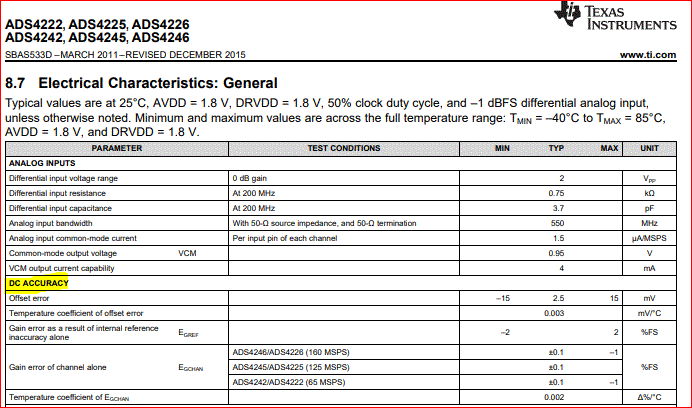
Regarding the DC accuracy section i see nothing that makes me having second thoughts. The input is Differential with a FS magnitude of 2Vpp and the input diff resistance is 750Ω @ 200MHz.

I understand that i have to build the front end accordingly with impedance matching etc.

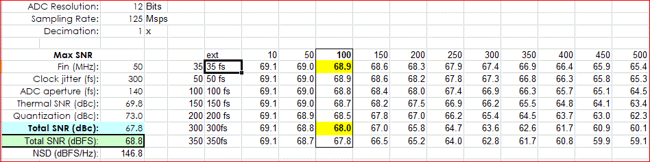
I went through your 12bit ADCs but all of them had a bandwidth many times greater than the sampling speed which if i am not mistaken means that they are targetting SDR.

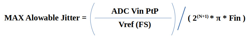
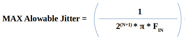
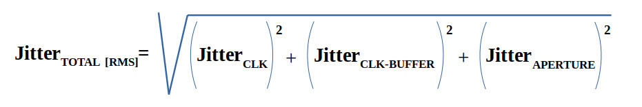
So, can a SDR ADC be used in a DSO and perform both in DC & AC coupling well?

Any suggestions? Parts?

Regards

Manos Tsachalidis

  • Hi Mano,

    Yes, most of our ADCs are suited for AC and DC coupling applications. Yes, wider input bandwidth does support higher IF applications like SDR, but can also be used for applications that don't required high input bandwidth.

    What sampling frequency are you looking to use? Is there a target specification that is very important to your application (SNR, low power, data output format, etc.)? 

    In the meantime, you can take a look at the ADC3224 family.

    Best Regards,

    Dan

  • High Dan,

    Thanks for the reply. The ADC i chose is probably the one i will be using because of its' parallel DDR LVDS output. I will be using a Cyclone IV E that is cheap but has LVDS transceivers that work higher than 400MBps. The one you proposed requires high speed transceiver > 1GBps which is too high and i do not want to go there. At least this is what i think... My experience is not that big with FPGAs so i am guessing. More or less the clock has also been chosen to be the 844N255I which does not require programming through SPI or I2C to output a 125MHz clock. Its' phase jitter is 300fS so i am (again) guessing that it will not affect the SNR of the 12bit ADC.

    The sampling frequency will be the max for the ADS4225 which is 125MHz.
    The bandwidth of the front end will most probably be between 100-150MHz

    My goal is to NOT affect the SNR of the ADC with the selection of the clock. I am considering using bandpass crystal filter at 124.8MHz which would greatly improve the clock jitter performance even more but i have not decided yet.

    Any suggestions?

    Regards
    Manos Tsachalidis
  • Hi Manos,

    We have a firmware example from our data capture platform that can help you get started with the FPGA design. Please take a look at the TSW1400EVM website ( www.ti.com/.../TSW1400EVM ) under the Software section. You will need Quartus (Altera / Intel FPGA design software) to open files.

    In regard to the clock jitter (300 fsec), you may want to consider that the aperture jitter of the ADS4225 is 140 fSec. This means that the clock jitter of 300 fsec may have some impact on the performance of the ADC (especially since there will be a "high" analog input frequency).

    TI offers an oscillator (no SPI or I2C, pin programmable) that can be programmed to 125 MHz with 100 to 200 fSec performance, LMK61PD0A2 . Did you have a need to drive several devices with the clock signal?

    Best Regards,

    Dan
  • Hi Dan and thanks again for your message,

    Yes you are right, my bad. The devices i am thinking of driving are a second ADS4225 as the target DSO is a quad channel.

    Also i want to drive that clock to the FPGA off course which will process the ADC data.

    The solution you are suggesting regarding the clock would be great if i was driving only one device.

    Would there be a chance to accomplish that (driving multiple devices from LMK61PD0A2) by using low noise high bandwidth opamps to distribute the signal across many devices or just use (better i think) a solution like the clock i have suggested BUT with better jitter performance?

    There is actually a formula that dictates the max jitter allowable for an ADC based on resolution (number of bits) and input signal frequency:

    This off course becomes, as follows, if the numerator is 1 or the input signal is just full scale:

    As i read, this formula calculates the value of jitter that will result in no more than 1/2 LSB (N+1) noise for the given params which are N=12bits & Fin=100MHz.

    The calculated value (max allowable jitter) was 389fs. Now if i solve for Fin=50MHz the max allowable jitter gets double the previous one: 777fs. What do you think?

    So, thinking that the clock i suggested has a 300fS which if combined with the ADC aperture jitter (140fS) gives me a total of 331fs => sqrt( CLKjiter^2 + APERTUREjitter^2) means that i am close to my target for 100MHz or 2 times lower for Fin=50MHz..

    Does TI have a similar clock solution so that i can feed at least 4 devices with the clock signal? I know that given the length of the signal traces they are considered as "transmission lines" and must be terminated accordingly.

    I know for a fact that in practice values will be a little worse and that is why the clock should be a little better than 300fs (for 100MHz).

    Can you pls suggest if i am doing this wrong? The truth is that i have been working as an engineer for 20 years but regarding high speed signalling and high speed ADCs, my experience is not that good.

    Please be kind to revert with any suggestions you might have.

    Regards

    Manos

  • Hi Manos,

    The ADS4225 also provides the Data Clock as an output that is aligned with the LVDS data, so you can use this to clock the data in to your FPGA. TI has clock fanout buffers (1 to 4, etc...) that have very low additive jitter. I have included our clocking team, so that they can help with selecting the right part for your application.

    In regard to the jitter, I would recommend looking at this presentation from one of our systems engineers.  

    Additionally, here is a good picture of how a higher clock jitter affects the SNR with increasing Fin.

    In your case, with a 300 fs clock input to the ADS4225 (and a 100 MHz Fin), SNR may decrease around 1 dBFS.

    Best Regards,

    Dan

  • Hi,

    I see a comment asking for us to recommend a fanout buffer.

    Have you considered the LMK00304 or LMK00334? This is a 4 output fanout buffer with differential outptus that requires no programming.

    Regards,
    Dean
  • Hi Dean and thanks for your msg,

    I think i have finally concluded which parts to use. I am focusing on clock oscillator LMK61E2-125M designed for 125MHz and the 4-LVPECL-output clock buffer CDCLVP1204.

    This started with me knowning almost nothing about what the challenges were when it comes to clocking a 12bit ADC.

    I went through a lot of TI app notes and i think now that things are much more clear.

    Finally i think that these part are the suitable candidates for not comprimizing the SNR of the the ADC ADS4225 that i have selected. 

    I really did not know at first that these parts even existed as i never got involved with the design of high speed stuff.

    So, talking to Dan, our last conversation was about me using a 4-output clock with a ~300fs RMS phase jitter which combined with the 140fs aperture jitter resulted in a ~330fs phase jitter which is close to the max allowable phase jitter that i calculated @ 380fs (Fin:100MHz).

    In order to improve the clock phase jitter performance i finally selected the LMK61E2-125M with a TYP 100fs @ 125MHz and CDCLVP1204 with an additive phase jitter of ~55fs. So considering this information i am well below the 330fs performance of my previously selected components.

    I have been also thinking about using very narrow ~20KHz crystal band-pass filters to further reduce jitter but that is (after searching a bit) difficult to find. Also slew rate would have to be improved due to the fact that the signal would end up being a pure sine.

    My questions regarding the currently (newly) selected compnents are:

    How do you add all phase jitter values of ADS4225 (aperture jitter: 140fs), LMK61E2-125M (100fs) and CDCLVP1204 (55fs). The word "additive" keeps me thinking...

    If i had to guess it would be this:

    Also regarding the ADC ADS4225, i have got a few questions:

    I am considering using the mux mode in the output which means that with a 125MHz clock, ADC's parallel B output would be 250MHz. I am a bit confused at this point... Can i use both mux mode to get both inputs in one parallel output and at the same time use DDR LVDS to pass the data to the FPGA? Using the FPGA's LVDS receivers would be the only way to pass that data into the FPGA, otherwise its' pins would only be capable of switching up to 90-100MHz

    As this ADC is going to be used as a DSO, i have to find an extremely low noise opamp with a high input impedance. Which one would you recommend?

    The input DC reference voltage is nowhere to find. Usually there is a pin where i can supply a high precission DC reference which defines the LSB level. However, i saw that 2Vpp is the max input voltage. Is that supposed to be considered the internal voltage reference?

    The input of the ADC (P53, 9.3.1.2) refers only to AC coupled topologies. I understand that this ADC is supposed to be used in SDR applications but shouldn't there be any references to DC coupling topologies? Would such an implementation pose a threat to the DC accuracy behaviour?

    Thanks again for the help.

    Manos

  • Hi Manos,

    It looks like you have a good clocking solution lined up. Dean, thank you for suggesting some parts.

    Yes, additive jitter can be calculated as shown in your equation. Also, see this bit from one of TI's presentations.

    After looking at the datasheet a little further, it is not recommended to use the MUX mode above 80 MSPS since (as you mentioned) the data rate is doubled. For CMOS output, this is a pretty high data rate, and I can imagine that signal integrity issues will start to arise.

    The DC midpoint is provided by the VCM pin on the ADC which provides +0.95VDC. Yes, the 2Vpp input tells us that the voltage reference is from 0V to 2V.

    For DC coupled applications, I most commonly see a differential amplifier driving the ADC analog inputs. TI offers a family of high speed amplifiers (THS4541 is very popular for our evaluation boards), so I will loop in our amplifier team to see if they can help you with a front end recommendation. If DC parameters are a concern, please look closely at the DC specifications.

    Best Regards,

    Dan