Other Parts Discussed in Thread: ADS54J20
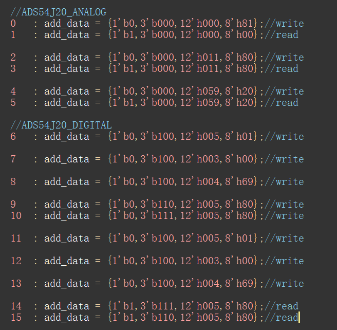
When the FPGA is used to configure the register of ADS54J20, SPI timing sequence is normal, SCK frequency is 1MHz, register readback of configured analog Bank is normal, and SPI readback fails when JESD Bank is configured. it seems that the SPI link is OK,and the analog bank working properly.
below is my FPGA code:
Is there any other incorrect configuration that could cause this problem ? power supply ? working mode ? (the PDN pin is pull down with 1K resistor just as the EVM board)
please help to check and Looking forward to your reply ASAP. thank you .
BR//


