This thread has been locked.

If you have a related question, please click the "Ask a related question" button in the top right corner. The newly created question will be automatically linked to this question.

DAC39J84EVM: Signal distortion from DAC

Part Number: DAC39J84EVM
Other Parts Discussed in Thread: DAC39J84

Hi,

I am using Xilinx FPGA KC705 to do DSP and transmit the processed signal together with I,Q signal by DAC39J84.

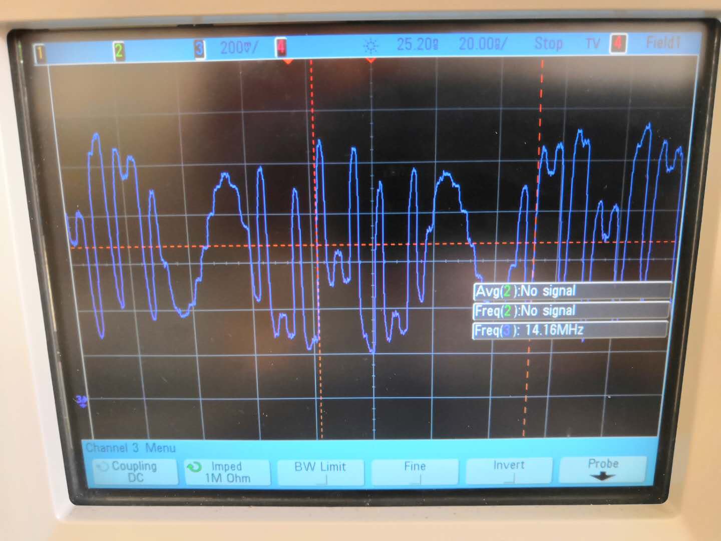
In the first stage, I plan to interface FPGA with DAC in JESD204 standard to transmit a sine wave. 

So far the link sync is achieved. But I received distorted signals from the DAC even though I matched all the configuration parameters.
LMFS =4221   K=16   I set these in DAC GUI

And I wrote the corresponding register values to JESD core in FPGA

Addr x008
Data x0000_0001 Enable Lane Alignment
Addr x00C
Data x0000_0000 [0] Disable Scrambling
Addr x020
Data x0000_0001 F (octets per frame) = 2
Addr x024
Data x0000_000F K (Frames per multi) = 16
Addr x014 Tx Only
Data x0000_0003 [7:0] ILA multiframes = 4
Addr x814 Tx Only
Data x000_0100 [12:8] s=1
Addr x810 ILA config 4
Data x0010_1004 [20:16] N'=16 [12:8] N=16 [7:0] M=4

Could anyone give me some suggestion about what could be the potential problems ?

Thanks for any help.

  • Hi Star_Li,

    We are taking a look into your issue, and will be back with you soon.

    Best Regards,

    Dan
  • Star,

    My guess is you are sending the wrong data on the lanes to the DAC. If you are using the DAC EVM GUI to program the DAC on your custom board, there is a good chance the serdes lanes crossbar switch could be programmed incorrectly. By default, the GUI will map the DAC input as follows:

    JESD Lane ID 3    RX0

    JESD Lane ID 2    RX1

    JESD Lane ID 1    RX2

    JESD Lane ID 0    RX3

    Regards,

    Jim 

  • Star,

    I also noticed you are attempting to use LMFS = 4221 mode. This is not a valid mode. You must use either 4211 mode (dual DAC mode) or 4421 (quad DAC mode).

    Regards,

    Jim

  • Hi Jim,

    Thanks for the reply. It is a typo. I want to say LMFS is 4421. That's how I program the JESD core. 

    Simply changing the sequence of the land ID doesn't work. I will send dc signals for different lanes and see how it goes.

    Thanks,

    Star

  • Hi Jim,

    In the datasheet of DAC, it shows a frame assembly table.

    I draw a doodle for the way I assembled the data. Is it correct?  LMFS=4421

    As for the parameter K, I set it to be 16 for JESD and DAC.

  • Star,

    This is a 16 bit DAC, not a 14 bit DAC like you are showing above. There is no CS = 2. The lower byte is 7:0 (1 octet, 8 bits).

    Regards,

    Jim

  • Hi Jim,

    I still can't get correct data even I used 16-bit sine wave LUT and no cs bits. 

    My transport layer is like this

    lane0_data_reg <= {signal0_sampl1[15:0], signal0_sampl0[15:0]};
    lane1_data_reg <= {signal1_sampl1[15:0], signal1_sampl0[15:0]};
    lane2_data_reg <= {signal2_sampl1[15:0], signal2_sampl0[15:0]};
    lane3_data_reg <= {signal3_sampl1[15:0], signal3_sampl0[15:0]};

    I tried to enable scrambling but it doesn't work either.

    The output data is like this now.

    I have a TSW14J10 card actually but I won't use it because I need customized firmware in the project.

    Do you have the register's values of JESD core in HSDC firmware? It would be better if I can have a look at how you set up JESD core in KC705 (LMF442) by the interposer card. Or could you please give me some other suggestions?

    Thanks,

    Star

  • TSW14J10KC705 DAC INI File Guide.docDAC3XJ84_LMF_442.iniStar,

    The JESD parameters used by the KC705 when I ran the 442 test are shown in the attached ini file. The FPGA used a core clock and reference clock that were the same frequency as the DAC clk. I have also attached a document that explains the ini file.

    Regards,

    Jim

  • 3683.JESD204_TI_reference_design.pdfStar,

    Here is another document they may help you.

    Regards,

    Jim

  • Appreciate for the help! I am looking into it.
  • Hi Jim,

    The data format in the ini file should be input data for spi instead of JESD. It’s weird even though all the settings are the same as the file in JESD ip core and DAC, I still can’t see correct data on the oscilloscope. I double checked all the register values of JESD as well.

    I connected the interposer card back to make sure the functionality of dac is good. I tried to transmit dc data say 7fff for channel 1, 5ffff for channel 2, 3fff for 3 and 1fff for 4. (Inductors and baluns are removed)But I saw 0v at the output. Any suggestions?

    Thanks,
    Star
  • Star,

    I would suggest looking at the example source code that can be found under the TSW14J10EVM product folder on the TI website and the examples that can be found on the Xilinx website. Have you tried using the Xilinx help website?

    Since you modified the DAC output circuit, to test the DAC output, you can use just the NCO. See attached file for how to do this. This requires no data from the FPGA.

    Regards,

    Jim

    6472.DAC38J84 100MHz NCO Test.pptx

  • Hi Jim,

    I find what the problem is, but I haven't figured out how to fix it yet.

    I generated 10 bits ramp signal, and the ramp signal was shown on the oscilloscope. However, the frequency was 4 times higher than expected. I assume the signal is saturated and goes back to 0. Then I tried 8 bits ramp signal and got expected signal and frequency. The signal is also in full swing.  Following that, I sent an 8-bit sine wave, and I got the correct signal.

    It seems the DAC can only consider the 8bits LSB of the 16 bits signal in my set up.

    To make sure, I tried to send several dc signals. Dc data 0x00FF (16'd255)is a full swing signal. 0x003F(16'd64) is 1/4 swing. 0x013F(16'd319) is also 1/4 swing. It makes sense if the DAC only takes the 8bits LSB because 64+255=319.  

    In DAC GUI, N and N' are set to be 16. I tried to change the values, but no matter what the values are, the output didn't change at all. I am also sure the N and N' in JESD IP core are 16 as well. 

    Do you know what causes the DAC to be only 8 bits resolution?

    Thanks,

    Star

  • Star,

    Please send me the screen shots of your GUI that are shown in the attached file. Before capturing the alarms screen shot, make sure to click on "Clear Alarms and Read" first. I want to see if you have any alarms present.

    Regards,

    Jim

    DAC39J84_442.pptx

  • The setting in the first three pages is as default. Thanks for the help.

    Star

  • Hi Jim,

    How can I interpret the alarms?

    Thanks,
    Star
  • Star,

    A bright green circle means an error. This will occur randomly on unused lanes. You have no alarms to worry about since you are only using lanes 0-3..

    Regards,

    Jim

  • It's weird that 8bits data becomes full swing and over that, the output of DAC will be saturated. Even though the resolution I set is 16 bits.

  • Star,

    Are you sending 2's comp data and have the DAC set for 2's comp format?

    Regards,

    Jim

  • I sent offset data and I had the DAC set for that.

    I sent 8 bits sine wave in the first photo and sent 16 bits sine wave in the second. They have the same setup. But the second one looks to be saturated.

  • Both are 16 bits data, but in the first case, I only use the 8lsb. 8 msb are set to be 0.
  • It is solved finally.
    The correct Fram assembly for 442 should be
    lane0_data_reg <= {signal0_sampl1[7:0],signal0_sampl1[15:8], signal0_sampl0[7:0],signal0_sampl0[15:8]};
    lane1_data_reg <= {signal1_sampl1[7:0],signal1_sampl1[15:8], signal1_sampl0[7:0],signal1_sampl0[15:8]};
    lane2_data_reg <= {signal2_sampl1[7:0],signal2_sampl1[15:8], signal2_sampl0[7:0],signal2_sampl0[15:8]};
    lane3_data_reg <= {signal3_sampl1[7:0],signal3_sampl1[15:8], signal3_sampl0[7:0],signal3_sampl0[15:8]};

    The information shown in Page 33 of dac39j84 datasheet is not correct.

    Thanks,
    Star